

herunterladen
APPLICATION BULLETIN
®
Mailing Address: PO Box 11400 • Tucson, AZ 85734 • Street Address: 6730 S. Tucson Blvd. • Tucson, AZ 85706
Tel: (602) 746-1111 • Twx: 910-952-111 • Telex: 066-6491 • FAX (602) 889-1510 • Immediate Product Info: (800) 548-6132
The need to glean AC signals from DC in the presence of
common-mode noise frequently occurs in signal condition-
ing applications. AC coupling to an instrumentation ampli-
fier (IA) or difference amplifier can be used to accurately
extract the AC signal while rejecting DC and common-mode
noise.
Adding capacitors and resistors to AC couple the inputs of
an instrumentation amplifier or difference amplifier seems
like an obvious approach for AC coupling, but it has prob-
lems. The DC restoration circuits shown in this bulletin have
the same transfer function but without the foibles.
Common-mode rejection of a difference amplifier depends
on extremely precise matching of input source impedance.
Adding RC networks to the inputs of either an IA or a
difference amplifier can significantly degrade the CMR,
especially for AC inputs. Even if the CMR is trimmed,
maintaining performance over temperature can be a prob-
lem.
The DC restoration circuits shown solve this problem by
placing a low-pass network in the feedback to the reference
pin of the IA or difference amplifier. The low-pass pole
translates into a high-pass function as referred to the input
with f
–3dB
= Gain/2•π•R•C. The Gain term refers to the Gain
from the reference pin to the output of the IA or difference
amplifier. The selection guide shows this Gain term as the
“High-pass multiplier”.
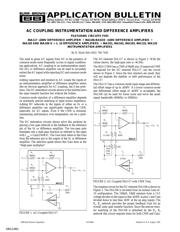
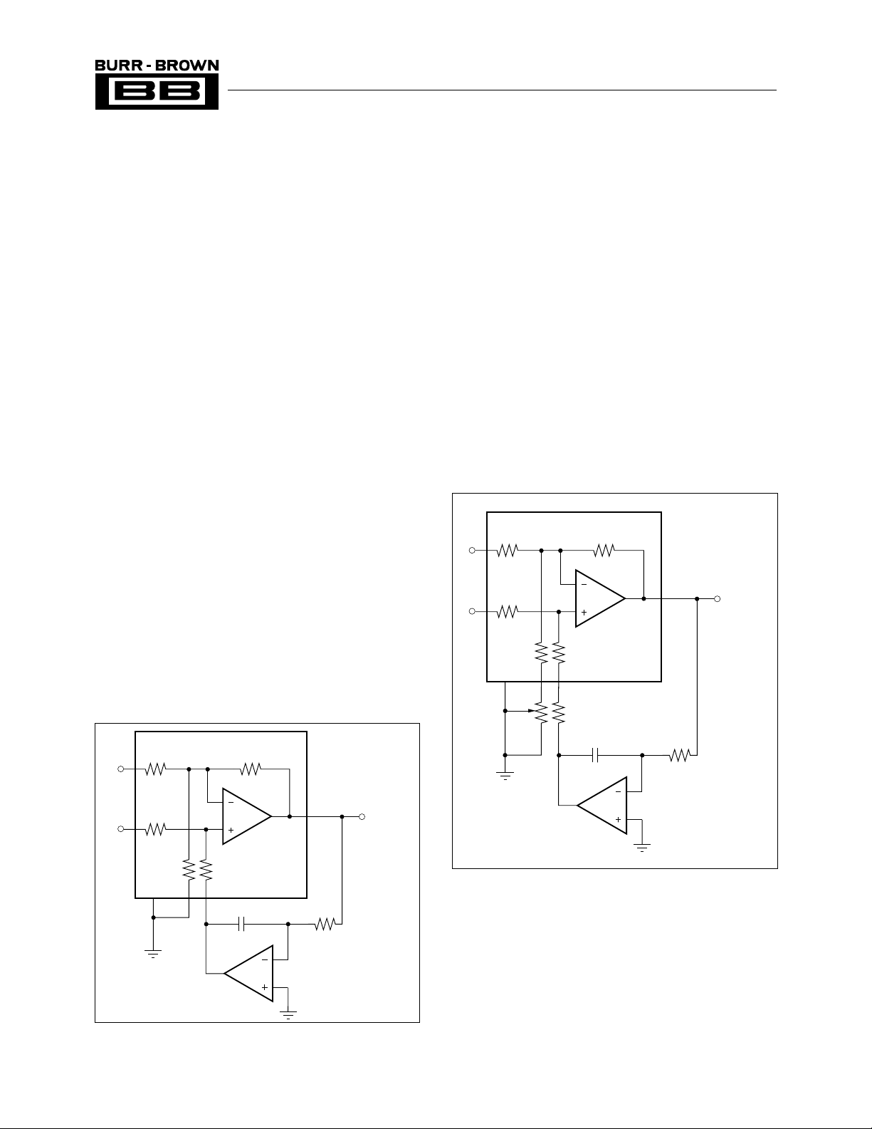
The DC-restored INA117 is shown in Figure 1. With the
values shown, the high-pass zero is ≈6.5Hz.
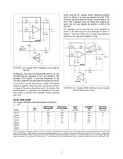
The INA117BM has a CMR of 86dB min. If improved CMR
is required for the DC restored INA117, use the circuit
shown in Figure 2. Since the trim resistors are small, they
will not degrade the stability or drift performance of the
INA117.
The INA117 has a common-mode input range and differen-
tial offset range of up to ±200V. If a lower common-mode
and differential offset range of ±100V is acceptable, the
INA106 can be used for lower noise and twice the small
signal bandwidth (400kHz vs 200kHz).
OPA602
380kΩ
V
2
R
1
380kΩ
R
2
V
3
2
3
380kΩ
R
3
6
21.1kΩ
R
5
20kΩ
R
4
815
C
1
0.47µF
1MΩ
R
1
INA117
V = V – V
OUT 3 2
10Ω
20
CMR
Trim
Ω
FIGURE 2. AC-Coupled INA117 with CMR Trim.
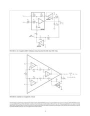
The simplest circuit for the DC-restored INA106 is shown in
Figure 3. The INA106 is reversed from its normal Gain-of-
10 configuration. The 100kΩ, 10kΩ resistors form a 11/1
voltage divider on the input so that ±100V at pins 1 and 5 are
divided down to less than ±10V at the op amp inputs. The
R
5
, R
6
network provides the proper feedback Gain for an
overall unity-gain transfer function. Since the precise resis-
tor matching of the INA106 is disturbed by the R
5
, R
6
network this circuit requires trims for both CMR and Gain.
AC COUPLING INSTRUMENTATION AND DIFFERENCE AMPLIFIERS
FEATURING CIRCUITS FOR:
INA117 ±200V DIFFERENCE AMPLIFIER • INA106-BASED ±100V DIFFERENCE AMPLIFIER •
INA105 AND INA106 G = 1, 10 DIFFERENCE AMPLIFIERS • INA101, INA102, INA103, INA110, INA120
INSTRUMENTATION AMPLIFIERS
By R. Mark Stitt (602) 746-7445
OPA602
380kΩ
V
2
R
1
380kΩ
R
2
V
3
2
3
380kΩ
R
3
6
21.1kΩ
R
5
20kΩ
R
4
815
C
1
0.47µF
1MΩ
R
1
INA117
V = V – V
OUT 3 2
FIGURE 1. AC-Coupled INA117.
1990 Burr-Brown Corporation AB-008A Printed in U.S.A. August, 1991
SBOA003