
herunterladen
LP3991
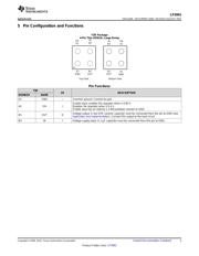
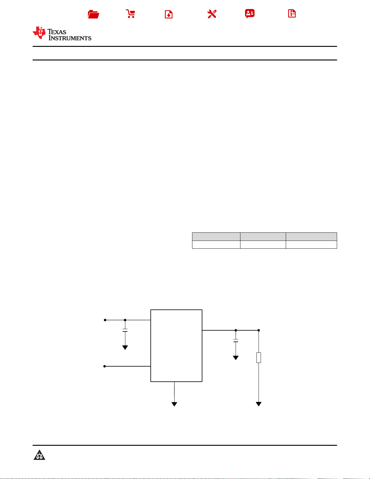
OUT
IN
1 PF
EN
GND
V
IN
Load
V
EN
B2
A2
A1
B1
C
OUT
*
C
IN
* For V
OUT
= 1.3 V or less,
C
OUT
may be reduced to 2.2 PF.
4.7 PF
Product
Folder
Sample &
Buy
Technical
Documents
Tools &
Software
Support &
Community
Reference
Design
LP3991
SNVS296I –DECEMBER 2006–REVISED AUGUST 2015
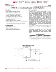
LP3991 300-mA Linear Voltage Regulator for Digital Applications
1 Features 3 Description
Operating from a minimum input voltage of 1.65 V,
1
• Input Voltage From 1.65 V to 4 V
the LP3991 regulator has been designed to provide
• Output Voltage From 0.8 V to 3 V
fixed stable output voltages for load currents up to
• 1% Accuracy at Room Temperature
300 mA. This device is suitable where accurate low
voltages are required from low input voltage sources
• 125-mV Dropout at 300-mA Load
and is therefore suitable for post regulation of
• 50-µA Quiescent Current at 1-mA Load
switched mode regulators. In such applications,
• Inrush Current Controlled to 600 mA
significant improvements in performance and EMI can
be realized, with little reduction in overall efficiency.
• PSRR 65 dB at 1 kHz
The LP3991 provides fixed outputs as low as 1.2 V
• 100-µs Start-Up Time for 1.5-V V
OUT
from a wide input range from 1.65 V to 4 V Using the
• Stable with Ceramic Capacitors as Small as 0402
enable (EN) pin, the device may be controlled to
• Thermal-Overload and Short-Circuit Protection
provide a shutdown state, in which negligible supply
current is drawn.
2 Applications
The LP3991 is designed to be stable with space-
• Post DC-DC Regulator saving ceramic capacitors as small as 0402 case
size.
• Battery Operated Devices
Performance is specified for a –40°C to 125°C
• Hand-Held Information Appliances
junction temperature range. For output voltage
options, contact your local Texas Instruments sales
office.
Device Information
(1)
PART NUMBER PACKAGE BODY SIZE (MAX)
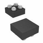
LP3991 DSBGA (4) 1.46 mm x 0.99 mm
(1) For all available packages, see the orderable addendum at
the end of the datasheet.
space
space
space
Typical Application Circuit
1
An IMPORTANT NOTICE at the end of this data sheet addresses availability, warranty, changes, use in safety-critical applications,
intellectual property matters and other important disclaimers. PRODUCTION DATA.
Verzeichnis
- ・ Konfiguration des Pinbelegungsdiagramms on Seite 3
- ・ Abmessungen des Paketumrisses on Seite 18 Seite 19 Seite 21 Seite 22 Seite 23
- ・ Markierungsinformationen on Seite 18 Seite 19
- ・ Blockdiagramm on Seite 9
- ・ Typisches Anwendungsschaltbild on Seite 1 Seite 11
- ・ Technische Daten on Seite 4
- ・ Anwendungsbereich on Seite 1 Seite 25
- ・ Elektrische Spezifikation on Seite 5 Seite 6