


herunterladen

Semiconductor Components Industries, LLC, 2011
November, 2011 − Rev. 6
1 Publication Order Number:
MBD701/D
MBD701,
MMBD701L,
SMMBD701L
Preferred Device
Silicon Hot-Carrier Diodes
Schottky Barrier Diodes
These devices are designed primarily for high−efficiency UHF and
VHF detector applications. They are readily adaptable to many other
fast switching RF and digital applications. They are supplied in an
inexpensive plastic package for low−cost, high−volume consumer
and industrial/commercial requirements. They are also available in a
Surface Mount package.
Features
Extremely Low Minority Carrier Lifetime − 15 ps (Typ)
Very Low Capacitance − 1.0 pF @ V
R
= 20 V
High Reverse Voltage − to 70 V
Low Reverse Leakage − 200 nA (Max)
AEC Qualified and PPAP Capable
S Prefix for Automotive and Other Applications Requiring Unique
Site and Control Change Requirements
Pb−Free Packages are Available*
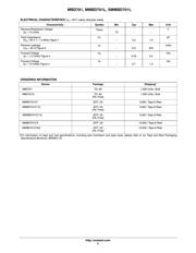
MAXIMUM RATINGS
Rating Symbol Value Unit
Reverse Voltage V
R
70 V
Forward Power Dissipation
@ T
A
= 25C
MBD701
MMBD701L, SMMBD701L
Derate above 25C
MBD701
MMBD701L, SMMBD701L
P
F
280
200
2.8
2.0
mW
mW/C
Operating Junction Temperature
Range
T
J
−55 to +125 C
Storage Temperature Range T
stg
−55 to +150 C
Stresses exceeding Maximum Ratings may damage the device. Maximum
Ratings are stress ratings only. Functional operation above the Recommended
Operating Conditions is not implied. Extended exposure to stresses above the
Recommended Operating Conditions may affect device reliability.
*For additional information on our Pb−Free strategy and soldering details, please
download the ON Semiconductor Soldering and Mounting Techniques Reference
Manual, SOLDERRM/D.
http://onsemi.com
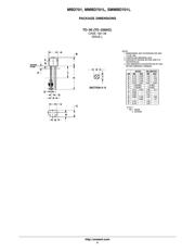
SOT−23 (TO−236)
CASE 318
STYLE 8
Preferred devices are recommended choices for future use
and best overall value.
*Date Code orientation and/or overbar may vary
depending upon manufacturing location.
1
5H M G
G
A = Assembly Location
Y = Year
WW = Work Week
5H = Device Code (SOT−23)
M = Date Code*
G = Pb−Free Package
(Note: Microdot may be in either location)
MARKING DIAGRAMS
3
CATHODE
1
ANODE
2
CATHODE
1
ANODE
TO−92 2−Lead
CASE 182
STYLE 1
MBD
701
AYWW G
G
SOT−23TO−92
SOT−23TO−92
See detailed ordering and shipping information in the package
dimensions section on page 2 of this data sheet.
ORDERING INFORMATION
Verzeichnis