
herunterladen

NPN General Purpose Amplifier
Transistor Surface Mount
MAXIMUM RATINGS (T
A
= 25°C)
Rating
Symbol Value Unit
Collector–Base Voltage V
(BR)CBO
60 Vdc
Collector–Emitter Voltage V
(BR)CEO
50 Vdc
Emitter–Base Voltage V
(BR)EBO
7.0 Vdc
Collector Current — Continuous I
C
500 mAdc
Collector Current — Peak I
C(P)
1.0 Adc
THERMAL CHARACTERISTICS
Characteristic Symbol Max Unit
Power Dissipation P
D
200 mW
Junction Temperature T
J
150 °C
Storage Temperature T
stg
–55 ~ +150 °C
ELECTRICAL CHARACTERISTICS (T
A
= 25°C)
Characteristic
Symbol Min Max Unit
Collector–Emitter Breakdown Voltage (I
C
= 10 mAdc, I
B
= 0) V
(BR)CEO
50 — Vdc
Collector–Base Breakdown Voltage (I
C
= 10 µAdc, I
E
= 0) V
(BR)CBO
60 — Vdc
Emitter–Base Breakdown Voltage (I
E
= 10 µAdc, I
C
= 0) V
(BR)EBO
7.0 — Vdc
Collector–Base Cutoff Current (V
CB
= 20 Vdc, I
E
= 0) I
CBO
— 0.1 µAdc
DC Current Gain
(1)
(V
CE
= 10 Vdc, I
C
= 150 mAdc)
(V
CE
= 10 Vdc, I
C
= 500 mAdc)
h
FE1
h
FE2
120
40
240
—
—
Collector–Emitter Saturation Voltage (I
C
= 300 mAdc, I
B
= 30 mAdc) V
CE(sat)
— 0.6 Vdc
Output Capacitance (V
CB
= 10 Vdc, I
E
= 0, f = 1.0 MHz) C
ob
— 15 pF
1. Pulse Test: Pulse Width ≤ 300 µs, D.C. ≤ 2%.
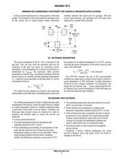
DEVICE MARKING
Marking Symbol
WR
X
The “X” represents a smaller alpha digit Date Code. The Date Code indicates the actual month
in which the part was manufactured.
Preferred devices are ON Semiconductor recommended choices for future use and best overall value.
ON Semiconductor
Semiconductor Components Industries, LLC, 2001
March, 2001 – Rev. 2
1 Publication Order Number:
MSD602–RT1/D
MSD602-RT1
ON Semiconductor Preferred Device
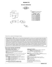
CASE 318D–04, STYLE 1
SC–59
2
1
3
COLLECTOR
3
2
BASE
1
EMITTER
Verzeichnis