
herunterladen
XAPP729 (v1.0.1) March 4, 2007 www.xilinx.com 1
© 2006–2007 Xilinx, Inc. All rights reserved. All Xilinx trademarks, registered trademarks, patents, and further disclaimers are as listed at http://www.xilinx.com/legal.htm.
PowerPC is a trademark of IBM, Inc. All other trademarks are the property of their respective owners.
NOTICE OF DISCLAIMER: Xilinx is providing this design, code, or information "as is." By providing the design, code, or information as one possible implementation of this feature,
application, or standard, Xilinx makes no representation that this implementation is free from any claims of infringement. You are responsible for obtaining any rights you may
require for your implementation. Xilinx expressly disclaims any warranty whatsoever with respect to the adequacy of the implementation, including but not limited to any warranties
or representations that this implementation is free from claims of infringement and any implied warranties of merchantability or fitness for a particular purpose.
Summary In today’s processor, digital signal processor (DSP), and other applications, memory data
widths can be 64 bits and higher. This application note shows how the 32-bit MicroBlaze™
processor can easily access these wide memories. This design is also suitable for use with the
IBM PowerPC™ (PPC405) processor because it connects to the On-chip Peripheral Bus
(OPB). The reference design provides a modification to an existing Xilinx EDK SDRAM
interface, enabling a 32-bit processor to access a 64-bit data bus.
Introduction When available solutions are too wide or narrow, custom memory width designs are created by
connecting standard memory devices together in parallel or serial configurations. This
application note describes the modifications to the standard EDK 32-bit wide SDRAM interface,
widening it to 64 bits. For the PPC405 or MicroBlaze processor, the connected memory
appears to be 32 bits wide, while in reality the memory is 64 bits wide. The reference design
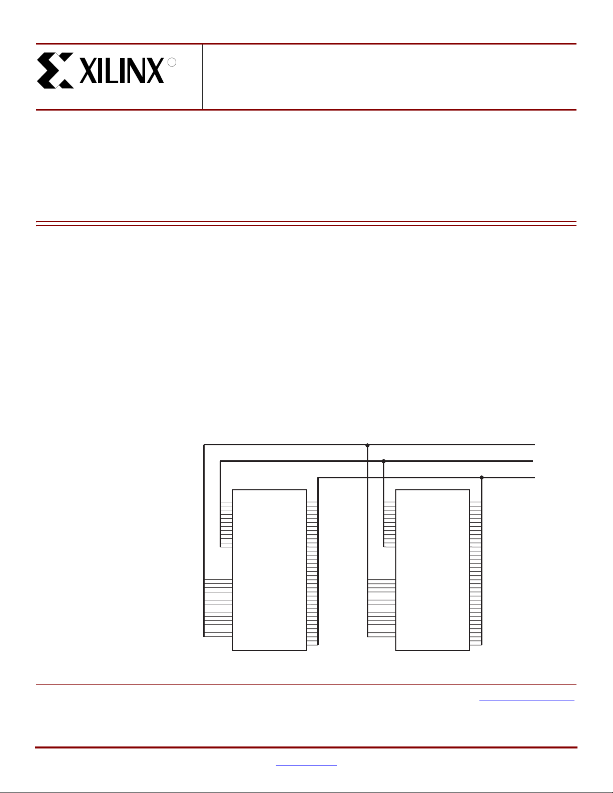
described in this application note uses two 32-bit SDRAMs configured in a 64-bit data setup.
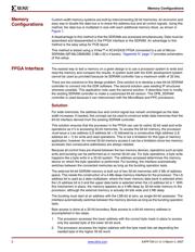
These memories share all control and address lines, as shown in Figure 1.
In this design, the memory is always accessed in 64-bit mode, using two consecutive memory
addresses from the processor. An access must first call the lower addressed 32-bit word
followed by the address of the higher 32-bit word.
The least-significant (LS) address bit is used as a multiplexer switch between even and odd
addresses to the memory. All lower 32-bit data is stored in one SDRAM bank, and the higher
32-bit data is stored in the second SDRAM block.
Application Note: Virtex-4 FPGA Family
XAPP729 (v1.0.1) March 4, 2007
Interfacing a 64-Bit DDR Memory Bus to a
32-Bit Microprocessor Bus
Author: Marc Defossez
R
Figure 1: 64-Bit Memory Setup
SDRAM_address [11:0]
SDRAM_control
SDRAM_data [31:0]
SDRAM_data [63:0]
SDRAM_data [63:32]
Micron
MT48LC8M32B2
SDRAM_2
Micron
MT48LC8M32B2
SDRAM_1
X729_01_010506