
herunterladen
AR
C
HIVE INF
O
RMATI
O
N
ARCHIVE INFORMATION
Replaced by MWIC930NR1(GNR1). There are no form, fit or function changes with this part
replacement. N suffix added to part number to indicate transition to lead-free terminations.
MWIC930R1 MWIC930GR1
1
RF Device Data
Freescale Semiconductor
RF LDMOS Wideband Integrated
Power Amplifiers
The MWIC930 wideband integrated circuit is designed for CDMA and
GSM/GSM EDGE applications. It uses Freescale’s newest High Voltage (26 to
28 Volts) LDMOS IC technology and integrates a multi -stage structure. Its
wideband On- Chip integral matching circuitry makes it usable from 790 to
1000 MHz. The linearity performances cover all modulations for cellular
applications: GSM, GSM EDGE, TDMA, N- CDMA and W-CDMA.
Final Application
• Typical Performance @ P1dB: V
DD
= 26 Volts, I
DQ1
= 90 mA, I
DQ2
=
240 mA, P
out
= 30 Watts P1dB, Full Frequency Band (921 -960 MHz)
Power Gain — 30 dB
Power Added Efficiency — 45%
Driver Application
• Typical Single-Carrier N - CDMA Performance: V
DD
= 27 Volts, I
DQ1
=
90 mA, I
DQ2
= 240 mA, P
out
= 5 Watts Avg., Full Frequency Band
(865- 894 MHz), IS -95 (Pilot, Sync, Paging, Traffic Codes 8 Through 13),
Channel Bandwidth = 1.2288 MHz. PAR = 9.8 dB @ 0.01%
Probability on CCDF.
Power Gain — 31 dB
Power Added Efficiency — 21%
ACPR @ 750 kHz Offset — -52 dBc in 30 kHz Bandwidth
• Capable of Handling 5:1 VSWR, @ 26 Vdc, 921 MHz, 30 Watts CW Output
Power
• Characterized with Series Equivalent Large-Signal Impedance Parameters
• On-Chip Matching (50 Ohm Input, DC Blocked, >4 Ohm Output)
• Integrated Quiescent Current Temperature Compensation with
Enable/Disable Function
• On-Chip Current Mirror g
m
Reference FET for Self Biasing Application
(1)
• Integrated ESD Protection
• 200°C Capable Plastic Package
• In Tape and Reel. R1 Suffix = 500 Units per 44 mm, 13 inch Reel.
1. Refer to AN1987/D, Quiescent Current Control for the RF Integrated Circuit Device Family. Go to http://www.freescale.com/rf.
Select Documentation/Application Notes - AN1987.
Document Number: MWIC930
Rev. 5, 5/2006
Freescale Semiconductor
Technical Data
746- 960 MHz, 30 W, 26-28 V
SINGLE N-CDMA, GSM/GSM EDGE
RF LDMOS WIDEBAND INTEGRATED
POWER AMPLIFIERS
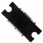
CASE 1329- 09
TO-272 WB - 16
PLASTIC
MWIC930R1
MWIC930R1
MWIC930GR1
CASE 1329A- 03
TO-272 WB - 16 GULL
PLASTIC
MWIC930GR1
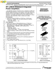
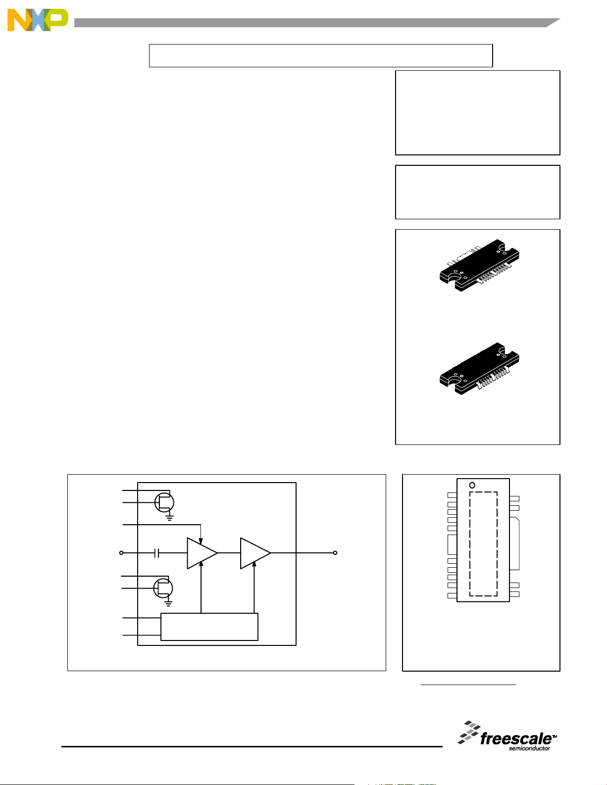
Figure 1. Functional Block Diagram Figure 2. Pin Connections
(Top View)
GND
V
RD1
RF
in
V
GS1
GND
V
RD2
RF
out/
V
DS2
GND
V
GS2
GND
V
RG2
V
DS1
V
RG1
NCNC
NC
V
GS1
RF
in
V
DS1
V
GS2
V
DS2
/RF
out
Quiescent Current
Temperature Compensation
V
RD2
V
RG2
2
3
4
5
6
7
8
16
15
14
13
12
9
10
11
1
Note: Exposed backside flag is source
terminal for transistors.
V
RD1
V
RG1
Freescale Semiconductor, Inc., 2006. All rights reserved.
Verzeichnis