


herunterladen
www.ti.com
FEATURES
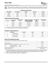
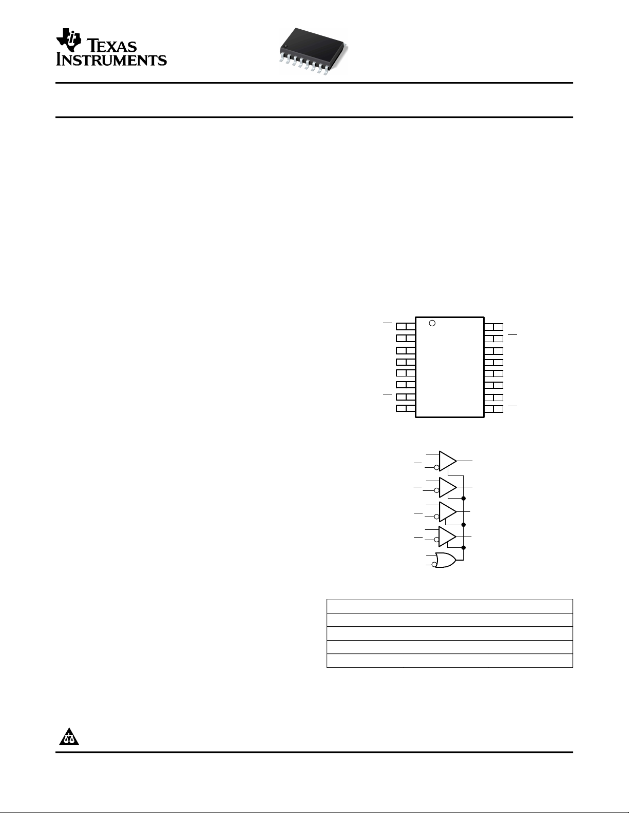
PIN ASSIGNMENTS
APPLICATIONS
1
2
3
4
5
6
7
8
16
15
14
13
12
11
10
9
AI
AI
AO
E1
BO
BI
BI
GND
VCC
DI
DI
DO
E2
CO
CI
CI
D PACKAGE
(TOP VIEW)
DESCRIPTION
AI
AO
BO
CO
DO
AIAI
BI
BI
C1
C1
D1
D1D1
E2
E1
ENABLE TRUTH TABLE
TB3R1, TB3R2
SLLS587B – NOVEMBER 2003 – REVISED MAY 2004
QUAD DIFFERENTIAL PECL RECEIVERS
The power-down loading characteristics of the re-
ceiver input circuit are approximately 8 kΩ relative to
• Low-Voltage Functional Replacements for the
the power supplies; hence they do not load the
Agere BRF1A, BRF2A, BRS2A, and BRS2B
transmission line when the circuit is powered down.
• Pin-Equivalent to General Trade 26LS32 De-
The package for these differential line receivers is the
vices
16-pin SOIC (D) package.
• High-Input Impedance Approximately 8 kΩ
The enable inputs of this device include internal
• 3.5-ns Maximum Propagation Delay
pullup resistors of approximately 40 kΩ that are
• TB3R1 Provides 50-mV Hysteresis
connected to V
CC
to ensure a logical high level input
if the inputs are open circuited.
• TB3R2 With -125-mV Threshold Offset for
Preferred State Output
• -0.5-V to 5.2-V Common Mode Range
• Single 3.3 V ±10% Supply
• Slew Rate Limited (0.5 ns min 80% to 20%)
• TB3R2 Output Defaults to Logic 1 When In-
puts Left Open or Shorted to V
CC
or GND
• ESD Protection HBM > 3 kV, CDM > 2 kV
• Operating Temperature Range: -40°C to 85°C
• Available SOIC (D) Package
• Digital Data or Clock Transmission Over Bal-
anced Lines
FUNCTIONAL BLOCK DIAGRAM
These quad differential receivers accept digital data
over balanced transmission lines. They translate
differential input logic levels to TTL output logic
levels.
The TB3R1 is a pin- and function-compatible replace-
ment for the Agere Systems BRF1A and BRF2A; it
includes 3-kV HBM and 2-kV CDM ESD protection.
The TB3R2 is a pin- and function-compatible replace-
ment for the Agere Systems BRS2A and BRS2B and
incorporates a -125-mV receiver input offset, pre-
ferred state output, 3-kV HBM and 2-kV CDM ESD
E1 E2 CONDITION
protection. The TB3R2 preferred state feature places
0 0 Active
the output in the high state when the inputs are open,
shorted to ground, or shorted to the power supply.
1 0 Active
0 1 Disabled
1 1 Active
Please be aware that an important notice concerning availability, standard warranty, and use in critical applications of Texas
Instruments semiconductor products and disclaimers thereto appears at the end of this data sheet.
PRODUCTION DATA information is current as of publication date.
Copyright © 2003–2004, Texas Instruments Incorporated
Products conform to specifications per the terms of the Texas
Instruments standard warranty. Production processing does not
necessarily include testing of all parameters.