


herunterladen

User's Guide
SNAU096A–July 2011–Revised October 2013
ADC14DC105EB and ADC12DC105EB Evaluation Boards
This User's guide applies to the ADC14DC105EB and ADC12DC105EB evaluation boards which are used
to evaluate the ADC14DC105 and ADC12DC105 A/D Converters, respectively. These ADCs belong to a
family of 12 and 14 bit converters that provide data at rates of up to 105MHz. Further reference in this
manual to the ADC14DC105 is meant to also include the other listed parts unless otherwise specified.
The evaluation board is designed to be used with the WaveVision5™ Data Capture Board which is
connected to a personal computer through a USB port and running WaveVision5™ software, operating
under Microsoft Windows. The software can perform an FFT on the captured data upon command and, in
addition to a frequency domain plot, shows dynamic performance in the form of SNR, SINAD, THD SFDR
and ENOB. The latest WaveVision 5 data capture board and WaveVision 5 Software is available through
the Texas Instruments website.
Contents
1 Board Assembly ............................................................................................................. 1
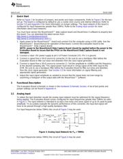
2 Quick Start ................................................................................................................... 3
3 Functional Description ...................................................................................................... 3
3.1 Analog Input ........................................................................................................ 3
3.2 ADC Reference Circuitry .......................................................................................... 4
3.3 ADC Clock Circuit .................................................................................................. 4
3.4 Digital Data Output ................................................................................................. 4
3.5 Data Format/Duty Cycle Stabilizer ............................................................................... 4
3.6 Power Supply Connections ....................................................................................... 4
4 Installing the ADC14DC105 Evaluation Board .......................................................................... 5
5 Evaluation Board Layout ................................................................................................... 6
6 Hardware Schematic ...................................................................................................... 10
7 Evaluation Board Bill of Materials ....................................................................................... 13
Appendix A ....................................................................................................................... 15
List of Figures
1 Major Component and Jumper Locations ............................................................................... 2
2 Test Set Up .................................................................................................................. 2
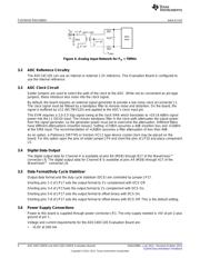
3 Analog Input Network for F
IN
> 70MHz................................................................................... 3
4 Analog Input Network for F
IN
< 70MHz................................................................................... 4
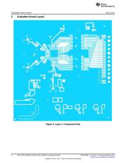
5 Layer 1: Component Side.................................................................................................. 6
6 Layer 2: Ground............................................................................................................. 7
7 Layer 3: Power .............................................................................................................. 8
8 Layer 4: Circuit Side........................................................................................................ 9
List of Tables
1 ADC12DC105/ADC14DC105 Evaluation Board BOM (rev 6)....................................................... 13
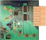
1 Board Assembly
The ADC14DC105 Evaluation Board comes pre-assembled. Refer to the Bill of Materials in Section 7 for a
description of components, to Figure 1 for major component placement and to Section 5 for the Evaluation
Board schematic.
1
SNAU096A–July 2011–Revised October 2013 ADC14DC105EB and ADC12DC105EB Evaluation Boards
Submit Documentation Feedback
Copyright © 2011–2013, Texas Instruments Incorporated
Verzeichnis