
herunterladen
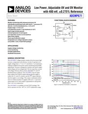
Low Power, Adjustable UV and OV Monitor
with 400 mV, ±0.275% Reference
Data Sheet
ADCMP671
Rev. 0
Information furnished by Analog Devices is believed to be accurate and reliable. However, no
responsibility is assumed by Analog Devices for its use, nor for any infringements of patents or other
rights of third parties that may result from its use. Specifications subject to change without notice. No
license is granted by implication or otherwise under any patent or patent rights of Analog Devices.
Trademarks and registered trademarks are the property of their respective owners.
One Technology Way, P.O. Box 9106, Norwood, MA 02062-9106, U.S.A.
Tel: 781.329.4700 www.analog.com
Fax: 781.461.3113 ©2011 Analog Devices, Inc. All rights reserved.
FEATURES
Window monitoring with minimum processor I/O
Individually monitoring N rails with only N + 1 processor I/O
400 mV, ± 0.275% threshold at V
DD
= 3.3 V, 25°C
Supply range: 1.7 V to 5.5 V
Low quiescent current: 17 μA maximum at 125°C
Input range includes ground
Internal hysteresis: 9.2 mV typical
Low input bias current: 2.5 nA maximum
Open-drain outputs
Power good indication output
Designated over voltage indication output
Low profile (1 mm), 6-lead TSOT package
APPLICATIONS
Supply voltage monitoring
Li-Ion monitoring
Portable applications
Handheld instruments
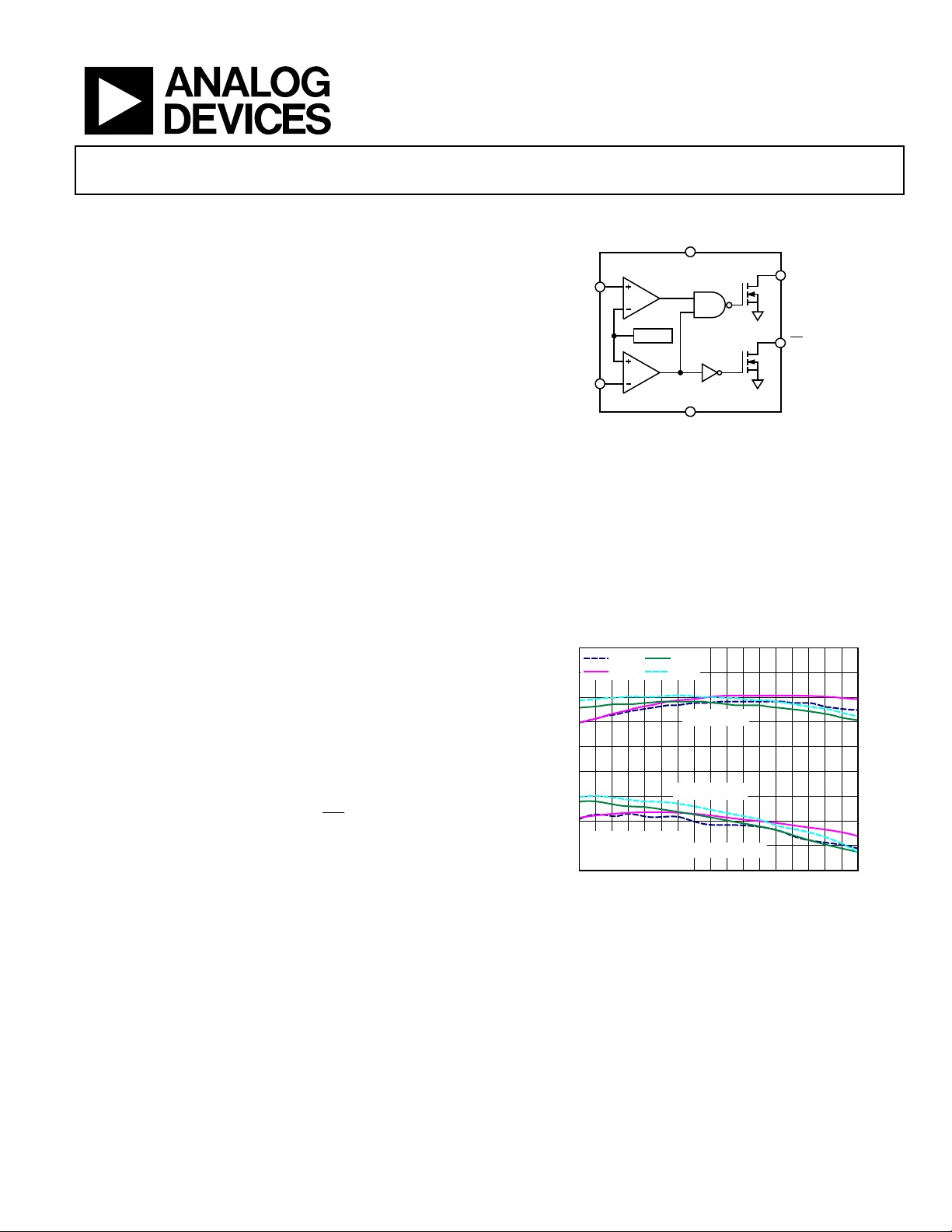
FUNCTIONAL BLOCK DIAGRAM
INH
UV
OV
INL
V
DD
GND
400mV
ADCMP671
PWRGD
OV
10160-001
Figure 1.
GENERAL DESCRIPTION
The ADCMP671 voltage monitor consists of two low power, high
accuracy comparators and reference circuits. It operates on a
supply voltage from 1.7 V to 5.5 V and draws 17 μA maximum,
making it suitable for low power system monitoring and portable
applications. The part is designed to monitor and report supply
undervoltage and overvoltage fault. The low input bias current
and voltage reference allows resistor adjustable UV and OV
threshold down to 400 mV. The ADCMP671 has two open-
drain outputs: the PWRGD output indicates that the supply is
within the UV and OV window, and the
OV
output indicates
that the supply is overvoltage. This output combination allows
users to window monitor N supplies with an N + 1 processor
input/output (I/O). Each output is guaranteed to sink greater
than 5 mA over temperature.
The ADCMP671 is available in 6-lead TSOT package. The
device operates over the −40°C to +125°C temperature range.
386
THRESHOLD VOLTAGE (mV)
TEMPERATURE (°C)
–40 –20 0 20 40 60 80 100 120
404
402
400
398
396
394
392
390
388
RISING INPUT
FALLING INPUT
INL2
INH2
INL1
INH1
TWO TYPICAL PARTS
COMPARATOR A AND COMPARATOR B
V
DD
= 5V
10160-002
Figure 2. Comparator Thresholds vs. Temperature
Verzeichnis
- ・ Konfiguration des Pinbelegungsdiagramms on Seite 8
- ・ Abmessungen des Paketumrisses on Seite 16
- ・ Teilenummerierungssystem on Seite 16
- ・ Blockdiagramm on Seite 1
- ・ Beschreibung der Funktionen on Seite 1 Seite 8
- ・ Technische Daten on Seite 1 Seite 3 Seite 7
- ・ Anwendungsbereich on Seite 1 Seite 14
- ・ Elektrische Spezifikation on Seite 9