

herunterladen
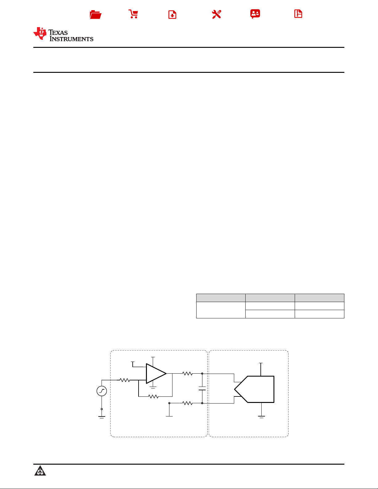
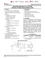
AVDD
AVDD
V
CM
4
1.8 nF
+
V
IN+
-
+
+
OPA836
AINP
AINM
GND
AVDD
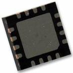
ADSxx53
4
INPUT DRIVER
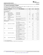
ADS8353 : 16-bit, 600 kSPS
ADS7853 : 14-bit, 1 MSPS
ADS7253 : 12-bit, 1 MSPS
1k
1 k
V
DC
Product
Folder
Sample &
Buy
Technical
Documents
Tools &
Software
Support &
Community
Reference
Design
ADS8353
,
ADS7853
,
ADS7253
SBAS584B –OCTOBER 2013–REVISED AUGUST 2014
ADSxx53 Dual, High-Speed, 16-, 14-, and 12-Bit,
Simultaneous-Sampling, Analog-to-Digital Converters
1 Features 2 Applications
1
• 16-, 14-, and 12-Bit, Pin-Compatible Family
• Motor Control:
Position Measurement Using Encoders
• Simultaneous Sampling of Two Channels
• Optical Networking: EDFA Gain Control Loops
• Supports Single-Ended and Pseudo-Differential
Inputs • Protection Relays
• High Speed: • Power Quality Measurement
• Three-Phase Power Controls
– ADS8353: 16 Bits, 600 kSPS
• Programmable Logic Controllers
– ADS7853: 14 Bits, 1 MSPS
– ADS7253: 12 Bits, 1 MSPS
3 Description
• Excellent DC Performance:
The ADS8353, ADS7853, and ADS7253 belong to a
– ADS8353:
family of pin-compatible, dual, high-speed,
– 16-Bit NMC DNL, ±2.5-LSB Max INL
simultaneous-sampling, analog-to-digital converters
(ADCs) that support single-ended and pseudo-
– ADS7853:
differential analog inputs.
– 14-Bit NMC DNL, ±2-LSB Max INL
Each device includes two individually programmable
– ADS7253:
reference sources that can be used for system-level
– 12-Bit NMC DNL, ±1-LSB Max INL
gain calibration. Also, a flexible serial interface that
• Excellent AC Performance:
can operate over a wide power-supply range enables
easy communication with a large variety of host
– ADS8353:
controllers. Power consumption for a given
– 89-dB SNR, –100-dB THD
throughput can be optimized by using the two low-
– ADS7853:
power modes supported by the device. All devices
are fully specified over the extended industrial
– 82-dB SNR, –90-dB THD
temperature range (–40°C to 125°C) and are
– ADS7253:
available in pin-compatible, WQFN-16 (3-mm ×
– 72-dB SNR, –90-dB THD
3-mm) and TSSOP-16 packages.
• Dual, Programmable, and Buffered
Device Information
(1)
2.5-V Internal Reference
PART NUMBER PACKAGE BODY SIZE (NOM)
• Fully-Specified Over the Extended Industrial
TSSOP (16) 5.00 mm × 4.40 mm
Temperature Range: –40°C to 125°C
ADSxx53
WQFN (16) 3.00 mm × 3.00 mm
• Small Footprint:
WQFN-16 (3-mm × 3-mm) and TSSOP-16
(1) For all available packages, see the orderable addendum at
the end of the datasheet.
Typical Application Diagram
1
An IMPORTANT NOTICE at the end of this data sheet addresses availability, warranty, changes, use in safety-critical applications,
intellectual property matters and other important disclaimers. PRODUCTION DATA.
Verzeichnis
- ・ Konfiguration des Pinbelegungsdiagramms on Seite 4
- ・ Abmessungen des Paketumrisses on Seite 62 Seite 64 Seite 65
- ・ Markierungsinformationen on Seite 62 Seite 63
- ・ Blockdiagramm on Seite 28
- ・ Typisches Anwendungsschaltbild on Seite 1 Seite 51 Seite 52
- ・ Technische Daten on Seite 5 Seite 11 Seite 40 Seite 42 Seite 43
- ・ Anwendungsbereich on Seite 1 Seite 51 Seite 52 Seite 71
- ・ Elektrische Spezifikation on Seite 6 Seite 7 Seite 8 Seite 9 Seite 10