herunterladen

AN1907
1
RF Application Information
Freescale Semiconductor
Solder Reflow Attach Method for High
Power RF Devices in Over-Molded Plastic
Packages
By: Keith Nelson, Quan Li, Lu Li, and Mahesh Shah
INTRODUCTION
The purpose of this application note is to provide
Freescale Semiconductor customers with a guideline for
solder reflow mounting of high power RF transistors and
integrated circuits in over-molded plastic (OMP) packages.
This document will aid customers in developing an assembly
process suitable for their design as well as their
manufacturing operation. Each Power Amplifier (PA) design
has its own unique performance requirements. Similarly,
each manufacturing operation also has its own process
capabilities. Therefore, each design and assembly may
require some fine-tuning. The intent of this application note
is to provide the information our customers need to establish
the process that is most suitable for their design and
compatible with their manufacturing operations.
When designing and manufacturing PA systems,
electrical, thermal, quality, and reliability factors must be
considered. Using the guidelines presented here, customers
should be able to develop a manufacturable assembly
process that can do the following:
• Create an interface that is thermally and electrically much
more conductive than thermal grease between the device
source contact and system ground.
• Provide a thermal ground that will conduct the dissipated
heat efficiently from the high power RF device to the
system sink.
• Develop a consistent electrical ground to provide a stable
RF performance over the life of the PA.
• Obtain a high quality solder joint between the device leads
and the solder pads on the printed circuit board (PCB) as
well as between the heat spreader of the device and the
carrier to ensure good field reliability.
• Maintain the package integrity during assembly as well as
in field use.
Throughout this application note, certain terminology is
used. Following are definitions of some of these terms.
TERMINOLOGY DEFINITIONS
• Base Transceiver Station (BTS) — A system making
cellular communication possible in a given cell.
• Carrier — Can either be pallet or coin. This metal piece
forms part of the thermal and electrical connection. The
carrier is attached to the PCB.
• Coin — A carrier that is smaller than the PCB.
• Flange or Heat Spreader — The exposed metal, primarily
copper, part of the OMP package. The die is attached to the
top of the heat spreader, and the exposed plated bottom is
soldered to the carrier.
• Heat Sink — The carrier that is typically attached to a finned
heat sink. The heat sink forms the part of the thermal path
that carries heat away from the device and to the cooling
air.
• Integrated Metal Carrier (IMC) — A metal pallet that is
bonded to the PCB.
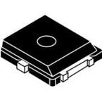
• Over- Molded Plastic (OMP) packages — A package
encapsulates the die and consists of a mold compound,
wire bonds, leads, and the heat spreader.
• Pallet — A carrier that is slightly larger than the PCB.
• Power Amplifier (PA) — An electronic assembly module
that takes in the input signal, amplifies the signal, and feeds
it to the antenna.
• Power Device — An RF Power device, usually an
Si- based LDMOS discrete device, a multi -stage IC
device, or a GaAs or GaN device.
• Printed Circuit Board (PCB) — The electrical
interconnection between the RF Power devices and other
electrical devices that are part of a PA.
AN1907
Rev. 3, 5/2009
Freescale Semiconductor
Application Note
Freescale Semiconductor, Inc., 2009. All rights reserved.
Verzeichnis


