


herunterladen
Product
Folder
Sample &
Buy
Technical
Documents
Tools &
Software
Support &
Community
LM10
SNOSBH4E –MAY 1998–REVISED OCTOBER 2015
LM10 Operational Amplifier and Voltage Reference
The circuit is recommended for portable equipment
1 Features
and is completely specified for operation from a
1
• Input Offset Voltage: 2 mV (Maximum)
single power cell. In contrast, high output-drive
• Input Offset Current: 0.7 nA (Maximum)
capability, both voltage and current, along with
thermal overload protection, suggest it in demanding
• Input Bias Current: 20 nA (Maximum)
general-purpose applications.
• Reference Regulation: 0.1% (Maximum)
The device is capable of operating in a floating mode,
• Offset Voltage Drift: 2 μV/°C
independent of fixed supplies. It can function as a
• Reference Drift: 0.002%/°C
remote comparator, signal conditioner, SCR controller
or transmitter for analog signals, delivering the
2 Applications
processed signal on the same line used to supply
power. It is also suited for operation in a wide range
• Remote Amplifiers
of voltage and current regulator applications, from low
• Battery-Level Indicators
voltages to several hundred volts, providing greater
• Thermocouple Transmitters
precision than existing ICs.
• Voltage and Current regulators
This series is available in the three standard
temperature ranges, with the commercial part having
3 Description
relaxed limits. In addition, a low-voltage specification
The LM10 series are monolithic linear ICs consisting
(suffix L) is available in the limited temperature
of a precision reference, an adjustable reference
ranges at a cost savings.
buffer and an independent, high-quality operational
amplifier.
Device Information
(1)
PART NUMBER PACKAGE BODY SIZE (NOM)
The unit can operate from a total supply voltage as
low as 1.1 V or as high as 40 V, drawing only 270 μA.
SOIC (14) 8.992 mm × 7.498 mm
A complementary output stage swings within 15 mV
LM10 SDIP (8) 8.255 mm × 8.255 mm
of the supply terminals or will deliver ±20-mA output
PDIP (8) 9.81 mm × 6.35 mm
current with ±0.4-V saturation. Reference output can
(1) For all available packages, see the orderable addendum at
be as low as 200 mV.
the end of the data sheet.
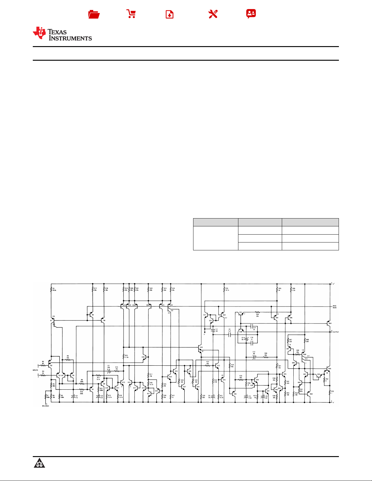
Operational Amplifier Schematic
(Pin numbers are for 8-pin packages)
1
An IMPORTANT NOTICE at the end of this data sheet addresses availability, warranty, changes, use in safety-critical applications,
intellectual property matters and other important disclaimers. PRODUCTION DATA.
Verzeichnis
- ・ Konfiguration des Pinbelegungsdiagramms on Seite 3
- ・ Abmessungen des Paketumrisses on Seite 30 Seite 32 Seite 33
- ・ Markierungsinformationen on Seite 30 Seite 31
- ・ Blockdiagramm on Seite 1 Seite 17
- ・ Typisches Anwendungsschaltbild on Seite 17 Seite 18
- ・ Technische Daten on Seite 4 Seite 17 Seite 27
- ・ Anwendungsbereich on Seite 1 Seite 17 Seite 37
- ・ Elektrische Spezifikation on Seite 5 Seite 6 Seite 7 Seite 8 Seite 9
- ・ Teilenummernliste on Seite 27