

herunterladen
LTC3876
1
3876f
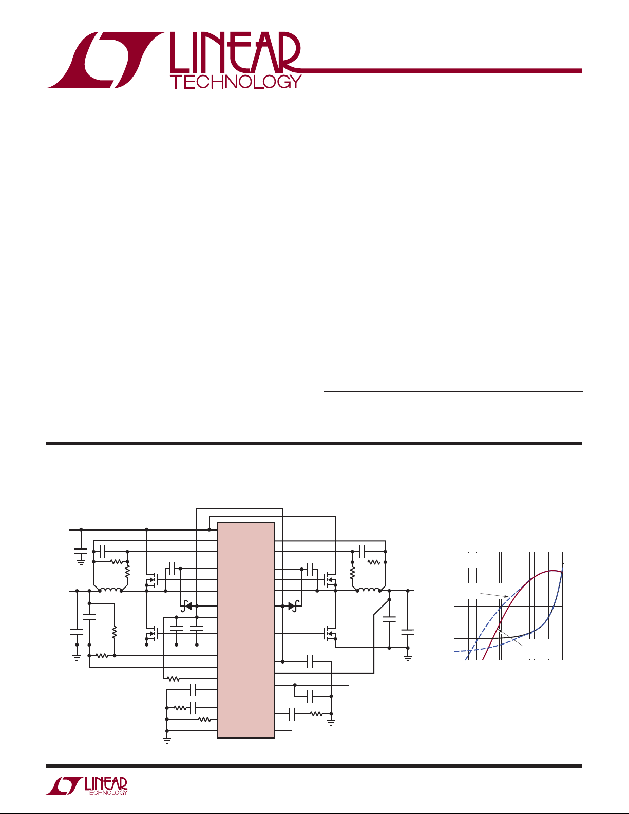
TYPICAL APPLICATION
FEATURES DESCRIPTION
Dual DC/DC Controller for
DDR Power with Differential VDDQ
Sensing and ±50mA VTT Reference
The LTC
®
3876 is a complete DDR power solution, com-
patible with DDR1, DDR2, DDR3 and future DDRX lower
voltage standards. The LTC3876 includes VDDQ and VTT
DC/DC controllers and a precision linear VTT reference. A
differential output sense amplifier and precision internal
reference combine to offer an accurate VDDQ supply. The
VTT controller tracks the precision VTTR linear reference
with less than 20mV total DC error. The precision VTTR
reference maintains 1.2% regulation accuracy tracking one-
half VDDQ over temperature for a ±50mA reference load.
The LTC3876 allows operation from 4.5V to 38V maximum
at the input. The VDDQ output can range from 1.0V to
2.5V, with a corresponding VTT and VTTR output range
of 0.5V to 1.25V. Voltage tracking soft-start, PGOOD and
fault protection features are provided.
DDR3 1.5V VDDQ/20A 0.75VTT/±10A 4.5V to 14V Input
APPLICATIONS
n
Complete DDR Power Solution with VTT Reference
n
Wide V
IN
Range: 4.5V to 38V, VDDQ: 1V to 2.5V
n
±0.67% VDDQ Output Voltage Accuracy
n
VDDQ and VTT Termination Controllers
n
±1.2% ±50mA Linear VTTR Reference Output
n
Controlled On-Time, Valley Current Mode Control
n
Frequency Programmable from 200kHz to 2MHz
Synchronizable to External Clock
n
t
ON(MIN)
= 30ns, t
OFF(MIN)
= 90ns
n
R
SENSE
or Inductor DCR Current Sensing
n
Power Good Output Voltage Monitor
n
Overvoltage Protection and Current Limit Foldback
n
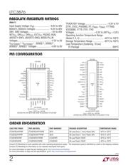
Thermally Enhanced 38-Pin (5mm × 7mm) QFN and
TSSOP Packages
n
Motherboard Memory
n
Servers
L, LT, LTC, LTM, Linear Technology, OPTI-LOOP, and the Linear logo are registered trademarks
and Hot Swap and No R
SENSE
are trademarks of Linear Technology Corporation. All other
trademarks are the property of their respective owners. Protected by U.S. Patents including
5481178, 5487554, 6580258, 6304066, 6476589, 6774611.
Efficiency/Power Loss
VDDR Channel 1
15k
3876 TA01a
1000pF
L2
0.47µH
VTT
0.75V
±10A
DB2
MT2
MB2
C
OUT4
330µF
3.57k
0.1µF
0.1µF
LTC3876
100k
VTTR
±50mA
100k
15k
V
IN
4.7µF
0.1µF
L1
0.47µH
V
IN
4.5V TO
14V
1.5V, 20A
VDDQ
20k
SENSE1
–
SENSE1
+
BOOST1
TG1
SW1
DRV
CC1
INTV
CC
DB1
MT1
3.57k
30.1k
15k
0.1µF
BG1
PGND
V
OUTSENSE1
+
V
OUTSENSE1
–
PGOOD
TRACK/SS1
ITH1
SGND
RT
SENSE2
–
SENSE2
+
BOOST2
TG2
SW2
DRV
CC2
BG2
VTTRVCC
VTTSNS
VTTR
ITH2
RUN
PGOOD
MB1
1µF
C
OUT1
100µF
C
OUT2
330µF
w2
0.1µF
1000pF
C
IN1
180µF
w2
1µF
15k
2.2µF
C
OUT3
100µF
LOAD CURRENT (A)
0.1
EFFICIENCY (%)
POWER LOSS (W)
90
100
110
3876 TA01b
60
50
40
80
70
4.0
4.5
1.5
0.5
1.0
0
3.0
3.5
2.5
2.0
FORCED
CONTINUOUS
MODE
DISCONTINUOUS
MODE
V
IN
= 12V
VDDQ = 1.5V
Verzeichnis
- ・ Konfiguration des Pinbelegungsdiagramms on Seite 10 Seite 11 Seite 12
- ・ Abmessungen des Paketumrisses on Seite 46
- ・ Paket-Footprint-Pad-Layout on Seite 46 Seite 47
- ・ Typisches Anwendungsschaltbild on Seite 1 Seite 13 Seite 14 Seite 15 Seite 16
- ・ Technische Daten on Seite 5
- ・ Anwendungsbereich on Seite 1 Seite 11 Seite 15 Seite 16 Seite 18
- ・ Elektrische Spezifikation on Seite 3 Seite 4 Seite 5 Seite 6 Seite 7