

herunterladen
© Semiconductor Components Industries, LLC, 2016
July, 2016 − Rev. 9
1 Publication Order Number:
MC100EL14/D
MC100EL14
5 V ECL 1:5 Clock
Distribution Chip
Description
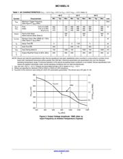
The MC100EL14 is a low skew 1:5 clock distribution chip designed
explicitly for low skew clock distribution applications. The V
BB
pin, an
internally generated voltage supply, is available to this device only.
For single-ended input conditions, the unused differential input is
connected to V
BB
as a switching reference voltage. V
BB
may also
rebias AC coupled inputs. When used, decouple V
BB
and V
CC
via a
0.01 mF capacitor and limit current sourcing or sinking to 0.5 mA.
When not used, V
BB
should be left open.
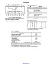
The EL14 features a multiplexed clock input to allow for the
distribution of a lower speed scan or test clock along with the high speed
system clock. When LOW (or left open and pulled LOW by the input
pulldown resistor) the SEL pin will select the differential clock input.
The common enable (EN
) is synchronous so that the outputs will only
be enabled/disabled when they are already in the LOW state. This
avoids any chance of generating a runt clock pulse when the device is
enabled/disabled as can happen with an asynchronous control. The
internal flip flop is clocked on the falling edge of the input clock,
therefore all associated specification limits are referenced to the
negative edge of the clock input.
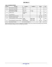
Features
• 50 ps Output-to-Output Skew
• Synchronous Enable/Disable
• Multiplexed Clock Input
• The 100 Series Contains Temperature Compensation
• PECL Mode Operating Range: V
CC
= 4.2 V to 5.7 V
with V
EE
= 0 V
• NECL Mode Operating Range: V
CC
= 0 V
with V
EE
= −4.2 V to −5.7 V
• Q Output will Default LOW with Inputs Open or at V
EE
• Internal Input Pull-down Resistors on All Inputs, Pull-up Resistors
on Inverted Inputs
• This Device is Pb-Free, Halogen Free and is RoHS Compliant
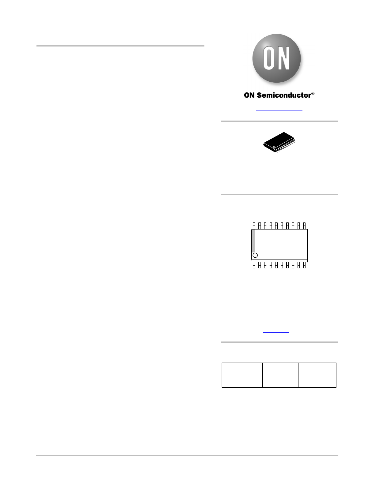
SOIC−20 WB
DW SUFFIX
CASE 751D−05
MARKING DIAGRAM
www.onsemi.com
A = Assembly Location
WL = Wafer Lot
YY = Year
WW = Work Week
G = Pb-Free Package
20
1
100EL14
AWLYYWWG
*For additional marking information, refer to
Application Note AND8002/D
.
ORDERING INFORMATION
Device Package Shipping
MC100EL14DWG
SOIC−20 WB
(Pb-Free)
38 Units/Tube
Verzeichnis
- ・ Konfiguration des Pinbelegungsdiagramms on Seite 2
- ・ Abmessungen des Paketumrisses on Seite 7
- ・ Paket-Footprint-Pad-Layout on Seite 7
- ・ Teilenummerierungssystem on Seite 1 Seite 8
- ・ Markierungsinformationen on Seite 1 Seite 6 Seite 8
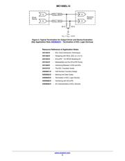
- ・ Typisches Anwendungsschaltbild on Seite 2
- ・ Teilenummernliste on Seite 3