Web Analytics
Datasheet
Teiledatenblatt > Microprocessor Development Kit > ON Semiconductor > NB4N11MDTEVB Datenblatt-PDF > NB4N11MDTEVB Benutzerreferenzhandbuch Seite 1/6
NB4N11MDTEVB
€ 266.79
Preis von AiPCBA

NB4N11MDTEVB Benutzerreferenzhandbuch - ON Semiconductor

  • Hersteller:
    ON Semiconductor
  • Kategorie:
    Microprocessor Development Kit
  • Fallpaket
    -
  • Beschreibung:
    Evaluation Board For NB4N11M
Aktualisierte Uhrzeit: 2025-04-23 11:23:17 (UTC+8)

NB4N11MDTEVB Benutzerreferenzhandbuch

Seite:von 6
PDF herunterladen
Neu laden
herunterladen
© Semiconductor Components Industries, LLC, 2012
February, 2012 Rev. 1
1 Publication Order Number:
EVBUM2071/D
NB4N11MDTEVB
Evaluation Board User's
Manual for NB4N11M
Description
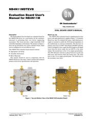
ON Semiconductor has developed an evaluation board for
the NB4N11M device as a convenience for the customers
interested in performing their own device engineering
assessment. This board provides a high bandwidth 50 W
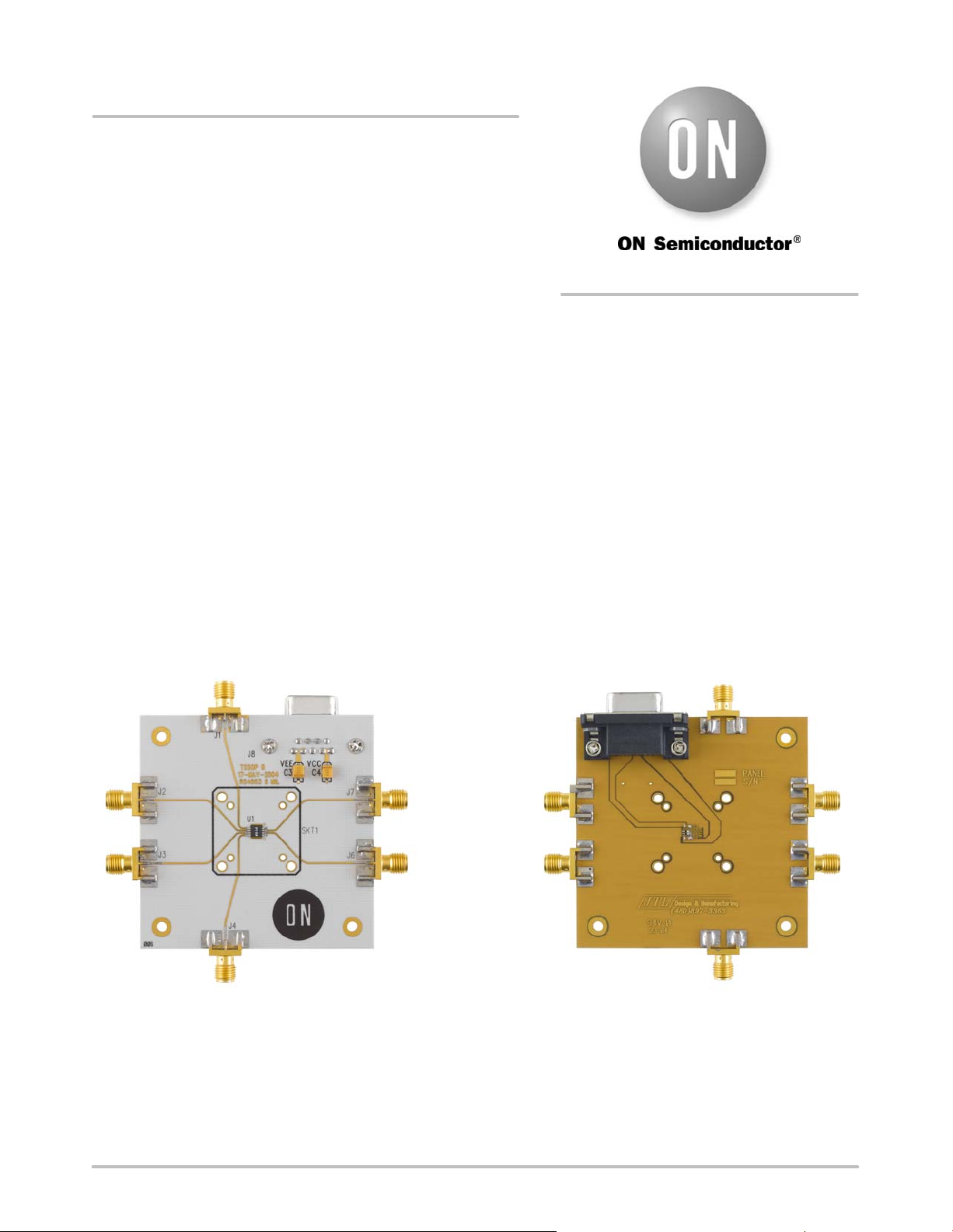
controlled impedance environment. The pictures in Figure 1
show the top and bottom view of the evaluation board, which
can be configured in several different ways.
This NB4N11M evaluation board manual contains:
Appropriate Lab Setup
Assembly Instructions
Bill of Materials
This manual should be used in conjunction with the
NB4N11M device data sheet, which contains full technical
details on the device specifications and operation.
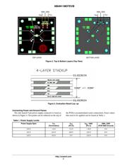
Board LayUp
The NB4N11M evaluation board is implemented in four
layers with split (dual) power supplies (Figure 7, Evaluation
Board Layup). For standard lab setup, a split (dual) power
supply is essential to enable the 50 W internal impedance in
the oscilloscope as a devices termination. The first layer or
primary trace layer is 0.005 thick Rogers RO4003 material,
which is designed to have equal electrical length on all signal
traces from the device under the test (DUT) to the sense
output. The second layer is the 1.0 oz copper ground plane.
The FR4 dielectric material is placed between second and
third layer and between third and fourth layer. The third
layer is also 1.0 oz copper ground plane. The fourth layer is
the secondary trace layer.
Top View Bottom View
Figure 1. Top and Bottom View of the NB4N11M Evaluation Board
http://onsemi.com
EVAL BOARD USER’S MANUAL

NB4N11MDTEVB Datenblatt-PDF

NB4N11MDTEVB Benutzerreferenzhandbuch
ON Semiconductor
6 Seiten, 261 KB

NB4N11 Datenblatt-PDF

NB4N111KMNG
Datenblatt PDF
ON Semiconductor
Clock Fanout Buffer 10Out 1IN 1:10 32Pin QFN EP Tube
NB4N111KMNR4G
Datenblatt PDF
ON Semiconductor
Clock Fanout Buffer 10Out 1IN 1:10 32Pin QFN EP T/R
NB4N11MDTG
Datenblatt PDF
ON Semiconductor
Multi Level Clock / Data Input to CML Receiver / Buffer / Translator, 2.5Gbps, 3.3V, TSSOP 8 3.0x3.0x0.95 mm, 100-TUBE
NB4N11MDTR2G
Datenblatt PDF
ON Semiconductor
Multi Level Clock / Data Input to CML Receiver / Buffer / Translator, 2.5Gbps, 3.3V, TSSOP 8 3.0x3.0x0.95 mm, 2500-REEL
NB4N1158DTR2G
Datenblatt PDF
ON Semiconductor
Link Replicator 28Pin TSSOP T/R
NB4N11SMNR2G
Datenblatt PDF
ON Semiconductor
Clock Fanout Buffer 4Out 16Pin QFN EP T/R
NB4N11SMNG
Anderes Datenblatt
ON Semiconductor
Clock Fanout Buffer 2Out 1IN 1:2 16Pin QFN EP Rail
NB4N1158DTG
Datenblatt PDF
ON Semiconductor
Link Replicator for Fibre Channel, Gigabit Ethernet, HDTV and SATA
NB4N11MDTEVB
Benutzerreferenzhandbuch
ON Semiconductor
Evaluation Board For NB4N11M
Datenblatt-PDF-Suche
Suche
100 Millionen Datenblatt-PDF, aktualisieren Sie mehr als 5.000 PDF-Dateien pro Tag.
Kontakt online
Bonnie - AiPCBA Sales Manager Online, vor 5 Minuten
Ihre E-Mail *
Nachricht *
Senden