
herunterladen
© Semiconductor Components Industries, LLC, 2012
February, 2012 − Rev. 2
1 Publication Order Number:
EVBUM2078/D
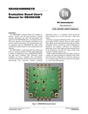
NB4N840MMNEVB
Evaluation Board User's
Manual for NB4N840M
Description
The NB4N840M Evaluation Board was designed to
provide a flexible and convenient platform to quickly
evaluate, characterize and verify the performance and
operation of the NB4N840M dual 2 x 2 Crosspoint Switch.
This user’s manual provides detailed information on the
board’s contents, layout and use. The manual should be used
in conjunction with the NB4N840M data sheet which
contains full technical details on device specifications and
operation.
The NB4N840M is a high−bandwidth fully differential
dual 2 x 2 crosspoint switch with CML inputs/outputs that
is suitable for applications such as SDH/SONET DWDM
and high speed switching. Fully differential design
techniques are used to minimize jitter accumulation,
crosstalk, and signal skew, which make this device ideal for
loop−through and protection channel switching
applications. Each 2 x 2 crosspoint switch can fan−out
and/or multiplex up to 3.2 Gb/s data and 2.7 GHz clock
signals.
Internally terminated differential CML inputs accept
AC−coupled LVPECL (Positive ECL) or direct coupled
CML signals. By providing internal 50 W input and output
termination resistor, the need for external components is
eliminated and interface reflections are minimized.
Differential 16 mA CML outputs provide matching internal
50 W terminations, and 400 mV output swings when
externally terminated, 50 W to V
CC
.
Single−ended LVCMOS/LVTTL SEL inputs control the
routing of the signals through the crosspoint switch which
makes this device configurable as 1:2 fan−out, repeater or
2 x 2 crosspoint switch. The device is housed in a low profile
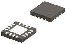
5 x 5 mm 32−pin QFN package.
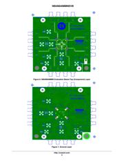
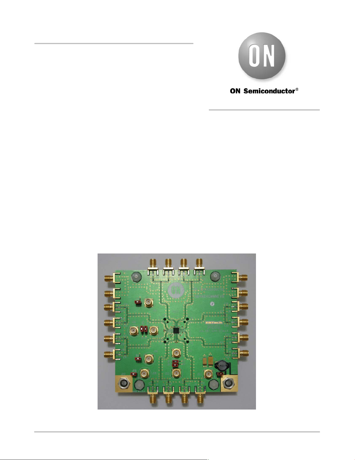
Figure 1. NB4N840M Evaluation Board
http://onsemi.com
EVAL BOARD USER’S MANUAL
Verzeichnis
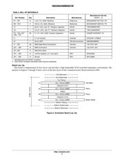
- ・ Teilenummerierungssystem on Seite 8
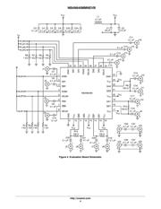
- ・ Blockdiagramm on Seite 4