
herunterladen
© Semiconductor Components Industries, LLC, 2009
July, 2009 − Rev. 3
1 Publication Order Number:
NCV33163/D
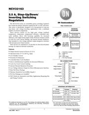
NCV33163
2.5 A, Step-Up/Down/
Inverting Switching
Regulators
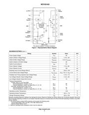
The NCV33163 series are monolithic power switching regulators
that contain the primary functions required for DC−to−DC converters.
This series is specifically designed to be incorporated in step−up,
step−down, and voltage−inverting applications with a minimum
number of external components.
These devices consist of two high gain voltage feedback
comparators, temperature compensated reference, controlled duty
cycle oscillator, driver with bootstrap capability for increased
efficiency, and a high current output switch. Protective features consist
of cycle−by−cycle current limiting, and internal thermal shutdown.
Also included is a low voltage indicator output designed to interface
with microprocessor based systems.
These devices are contained in a 16 pin dual−in−line heat tab plastic
package for improved thermal conduction.
Features
• Output Switch Current in Excess of 2.0 A
• Operation from 2.5 V to 60 V
OC
Input
• Low Standby Current
• Precision 2% Reference
• Controlled Duty Cycle Oscillator
• Driver with Bootstrap Capability for Increased Efficiency
• Cycle−by−Cycle Current Limiting
• Internal Thermal Shutdown Protection
• Low Voltage Indicator Output for Direct Microprocessor Interface
• Heat Tab Power Package
• Moisture Sensitivity Level (MSL) Equals 1
• Pb−Free Packages are Available*
• NCV Prefix for Automotive and Other Applications Requiring Site
and Change Controls
*For additional information on our Pb−Free strategy and soldering details, please
download the ON Semiconductor Soldering and Mounting Techniques
Reference Manual, SOLDERRM/D.
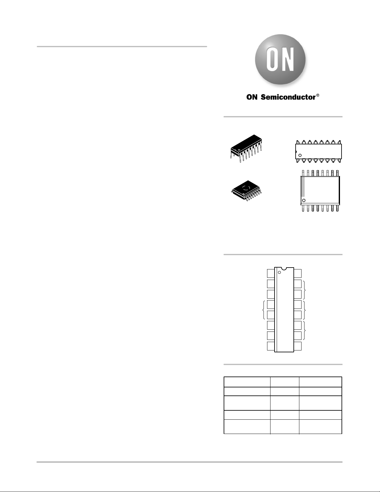
Device Package Shipping
†
ORDERING INFORMATION
NCV33163P PDIP−16 25 Units / Rail
NCV33163DWR2 SO−16WB 1000 Tape & Reel
MARKING
DIAGRAMS
A = Assembly Location
WL = Wafer Lot
YY = Year
WW = Work Week
G = Pb−Free Package
1
16
PDIP−16
P SUFFIX
CASE 648C
1
16
SO−16WB
DW SUFFIX
CASE 751G
1
16
116
15
14
13
12
11
10
9
2
3
4
5
6
7
8
(Top View)
LVI Output
Voltage Feedback 2
Voltage Feedback 1
GND
Timing Capacitor
V
CC
I
pk
Sense
Bootstrap Input
Switch
Emitter
GND
Switch Collector
Driver Collector
PIN CONNECTIONS
NCV33163P
AWLYYWWG
http://onsemi.com
†For information on tape and reel specifications,
including part orientation and tape sizes, please
refer to our Tape and Reel Packaging Specifications
/
NCV33163DWR2G SO−16WB
(Pb−Free)
1000 Tape & Reel
NCV33163PG PDIP−16
(Pb−Free)
25 Units / Rail
16
1
NCV33163DW
AWLYYWWG
Verzeichnis
- ・ Konfiguration des Pinbelegungsdiagramms on Seite 1
- ・ Abmessungen des Paketumrisses on Seite 14 Seite 15
- ・ Teilenummerierungssystem on Seite 1 Seite 15
- ・ Markierungsinformationen on Seite 1
- ・ Blockdiagramm on Seite 2 Seite 7 Seite 8
- ・ Technische Daten on Seite 1
- ・ Anwendungsbereich on Seite 1 Seite 9
- ・ Elektrische Spezifikation on Seite 3