
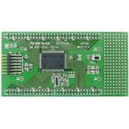

RL78/G13(512KB FLASH) ターゲット・ボード
QB-R5F100SL-TB ユーザーズ・マニュアル
ユーザーズ・マニュアル
R20UT0827XJ0200
Rev. 2.00 2013.06.28
本製品は、ルネサス エレクトロニクス製のプログラミング機能付きオンチップ・デバッグ・エミュレータ E1 を使用して、マイコンの動作を試
すためのターゲット・ボードです。
①RL78/G13 ターゲット・ボード(QB-R5F100SL-TB)の特徴
●RL78/G13(R5F100SL)搭載
●20MHz と 32.768KHz の発振子を搭載
●ユニバーサル・エリア(2.54mm ピッチ)を搭載
●フラッシュ・メモリ・プログラミング、オンチップ・デバッグに両対応(TOOL0 端子使用)
●マイコンの端子を周辺ボード・コネクタに配置した高拡張性
●鉛(Pb)フリー対応品
②ハードウエア仕様
CPU R5F100SL メイン・クロック動作周波数 20MHz(ボード上の発振子を使う場合)
CN1,CN2: 周辺ボードコネクタ(2.54mm ピッチ) 64pin ソケット x2(パッドのみ)
FP1: 14pin コネクタ(E1 接続用)
Power LED: 赤 x1(LED3)
評価用 LED: 黄 x2(LED1 は P76,LED2 は P77 へ接続)
評価用 SW: SW1(INTP0 へ接続)
メイン・クロック(OSC1): 20MHz 発振子(X1,X2 へ接続)
搭載部品
サブクロック(OSC2): 32.768KHz 発振子(XT1,XT2 へ接続)
動作電圧 2.7V~5.5V(OSC1:20MHz 発振子使用時)
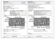
③寸法、部品配置など
109.22mm
EVDD
GND
QB-R5F100SL-TB(e)
1
2
64
63
55.88mm
OCD/Flash Program
1
CN3
SS-77195 JAPAN
13
VDD
10
20
30
40
1
2
CN1
SW1
CN1
メイン・クロック
サブクロック
Power LED
評価用LED
上:LED1
下:LED2
CN2
ユニバーサル・エリア
P77 LED2
LED1
P76
LED3
RL78/G13
(512KB)
50
60
30
40
20
10
CN2
64
63
50
60
OSC2
P124
P123
OSC1
20MHz
X1
P121
P122
X2
XT1
XT2
45.72mm
14pinコネクタ
GND
評価用SW
109.22mm
EVDD
GND
QB-R5F100SL-TB(e)
1
2
64
63
55.88mm
OCD/Flash Program
1
CN3
SS-77195 JAPAN
13
VDD
10
20
30
40
1
2
CN1
SW1
CN1
メイン・クロック
サブクロック
Power LED
評価用LED
上:LED1
下:LED2
CN2
ユニバーサル・エリア
P77 LED2
LED1
P76
LED3
RL78/G13
(512KB)
RL78/G13
(512KB)
50
60
30
40
20
10
CN2
64
63
50
60
OSC2
P124
P123
OSC1
20MHz
X1
P121
P122
X2
XT1
XT2
OSC2
P124
P123
OSC1
20MHz20MHz
X1
P121
P122
X2
XT1
XT2
45.72mm
14pinコネクタ
GND
評価用SW
基板上のパターン
について:パターンをカットすることで、その回路はオープンとなります。
再度接続させたい場合は半田ショートしてください。
P76,P77 を使用する場合は LED の左のショートパッドをパターンカットしてください。
回路図のパッドの表示 オープン:
ショート:
④使用上の注意
・本製品に関してのサポートはお受けしておりません。初期不良の場合に限り、交換いたします。
R20UT0827XJ0200 Rev.2.00 Page 1 of 2
2013.06.28
RL78/G13(512KB FLASH) Target board
QB-R5F100SL-TB User’s Manual
User’s Manual
R20UT0827XJ0200
Rev. 2.00 2013.06.28
The QB-R5F100SL-TB is a target board used for evaluating microcontroller operations, using the E1, Renesas Electronics on-chip
debug emulator with programming function (hereinafter referred to as E1).
(1) RL78/G13
target board (QB-R5F100SL-TB) features
● Built-in RL78/G13 (R5F100SL).
● A 20 MHz resonator and a 32.768KHz resonator are mounted.
● Equipped with universal area (2.54 mm pitch)
●Supports both flash memory programming and on-chip debugging (using TOOL0 pin)
● Highly extendable; peripheral board connectors are equipped with microcontroller pins
● Lead-free (Pb-free) product
(2) hardware specifications
CPU R5F100SL Main clock operating frequency 20 MHz(when use resonator mounted on board)
CN1, CN2: Peripheral board connectors (2.54 mm pitch), 64-pin socket 2 (pad only)
FP1: 14-pin connector (for E1 connection)
Power LED: Red 1 (LED3)
Test LED: Yellow 2 (LED1 connected to P76, LED2 connected to P77)
Test SW: SW1 (connected to INTP0)
Main clock (OSC1): 20 MHz oscillator (connected to X1 and X2)
Embedded parts
Subclock (OSC2): 32.768 KHz oscillator (connected to XT1 and XT2)
Operating voltage 2.7 to 5.5 V(when 20 MHz oscillator used at OSC1)
(3) Dimensions and parts layout
109.22mm
EVDD
GND
QB-R5F100SL-TB(e)
1
2
64
63
55.88mm
OCD/Flash Program
1
CN3
SS-77195 JAPAN
13
VDD
10
20
30
40
1
2
CN1
SW1
CN1
Main Clock
Sub Clock
Power LED
Test LED
upper:LED1
lower:LED2
CN2
Universal area
P77 LED2
LED1
P76
LED3
RL78/G13
(512KB)
50
60
30
40
20
10
CN2
64
63
50
60
OSC2
P124
P123
OSC1
20MHz
X1
P121
P122
X2
XT1
XT2
45.72mm
14pin connector
GND
Test SW
109.22mm
EVDD
GND
QB-R5F100SL-TB(e)
1
2
64
63
55.88mm
OCD/Flash Program
1
CN3
SS-77195 JAPAN
13
VDD
10
20
30
40
1
2
CN1
SW1
CN1
Main Clock
Sub Clock
Power LED
Test LED
upper:LED1
lower:LED2
CN2
Universal area
P77 LED2
LED1
P76
LED3
RL78/G13
(512KB)
RL78/G13
(512KB)
50
60
30
40
20
10
CN2
64
63
50
60
OSC2
P124
P123
OSC1
20MHz
X1
P121
P122
X2
XT1
XT2
OSC2
P124
P123
OSC1
20MHz20MHz
X1
P121
P122
X2
XT1
XT2
45.72mm
14pin connector
GND
Test SW
Pattern on the board:
Splitting this wiring leaves open the relevant circuit ( ).
To reconnect the circuit, short the circuit by soldering (
).
When using P76 and P77, cut off the short pad on the right side of LED.
Showing of the pad on circuit diagram. open:
short:
(4) Notes on use
● Renesas Electronics will not provide any support for this board, but the board can be exchanged with a new product only when
it has an initial failure.
R20UT0827XJ0200 Rev.2.00 Page 1 of 2
2013.06.28