


herunterladen
SCAS813A − AUGUST 2005 − REVISED DECEMBER 2005
1
POST OFFICE BOX 655303 • DALLAS, TEXAS 75265
D Low Jitter Clock Multiplier by x4, x6, x8.
Input Frequency Range (19 MHz to
125 MHz). Supports Output Frequency
From 150 MHz to 500 MHz
D Fail-Safe Power Up Initialization
D Low Jitter Clock Divider by /2, /3, /4. Input
Frequency Range (50 MHz to 125 MHz).
Supports Ranges of Output Frequency
From 12.5 MHz to 62.5 MHz
D 2.6 mUI Programmable Bidirectional Delay
Steps
D Typical 8-ps Phase Jitter (12 kHz to 20 MHz)
at 500 MHz
D Typical 2.1-ps RMS Period Jitter (Entire
Frequency Band) at 500 MHz
D One Single-Ended Input and One
Differential Output Pair
D Output Can Drive LVPECL, LVDS, and
LVTTL
D Three Power Operating Modes to Minimize
Power
D Low Power Consumption (Typical 200 mW
at 500 MHz)
D Packaged in a Shrink Small-Outline
Package (DBQ)
D No External Components Required for PLL
D Spread Spectrum Clock Tracking Ability to
Reduce EMI
D Applications: Video Graphics, Gaming
Products, Datacom, Telecom
D Accepts LVCMOS, LVTTL Inputs for
REFCLK Terminal
D Accepts Other Single-Ended Signal Levels
at REFCLK Terminal by Programming
Proper V
DD
REF Voltage Level (For
Example, HSTL 1.5 if V
DD
REF = 1.6 V)
D Supports Industrial Temperature Range of
−40
°
C to 85
°
C
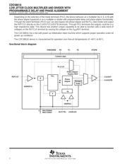
description
The CDC5801A device provides clock multiplication and division from a single-ended reference clock
(REFCLK) to a differential output pair (CLKOUT/CLKOUTB). The multiply and divide terminals (MULT/DIV0:1)
provide selection for frequency multiplication and division ratios, generating CLKOUT/CLOUTKB frequencies
ranging from 12.5 MHz to 500 MHz with a clock input reference (REFCLK) ranging from 19 MHz to 125 MHz.
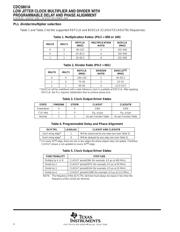
See Table 1 and Table 2 for detail frequency support.
The implemented phase aligner provides the possibility to phase align (zero delay) between
CLKOUT/CLKOUTB and REFCLK or any other CLK in the system by feeding the clocks that need to be aligned
to the DLYCTRL and the LEADLAG terminals.
The phase aligner also allows the user to delay or advance the CLKOUT/CLKOUTB with steps of 2.6 mUI (unit
interval). For every rising edge on the DLYCTRL terminal, the output clocks are delayed by 2.6-mUI step size
as long as there is low on the LEADLAG terminal. Similarly, for every rising edge on the DLYCTRL terminal, the
output clocks are advanced by 2.6-mUI step size as long as there is high on the LEADLAG terminal. The
CDC5801A has a fail-safe power up initialization state-machine which supports proper operation under all
power up conditions. As the phase between REFCLK and CLKOUT/CLKOUTB is random after power up, the
application may implement a self calibration routine at power up to produce a certain phase start position, before
programming a fixed delay with the clock on the DLYCTRL terminal.
Copyright 2005, Texas Instruments Incorporated
!"# $ %&'# "$ (&)*%"# +"#',
+&%#$ %! # $('%%"#$ (' #-' #'!$ '."$ $#&!'#$
$#"+"+ /""#0, +&%# (%'$$1 +'$ # '%'$$"*0 %*&+'
#'$#1 "** (""!'#'$,
Please be aware that an important notice concerning availability, standard warranty, and use in critical applications of
Texas Instruments semiconductor products and disclaimers thereto appears at the end of this data sheet.
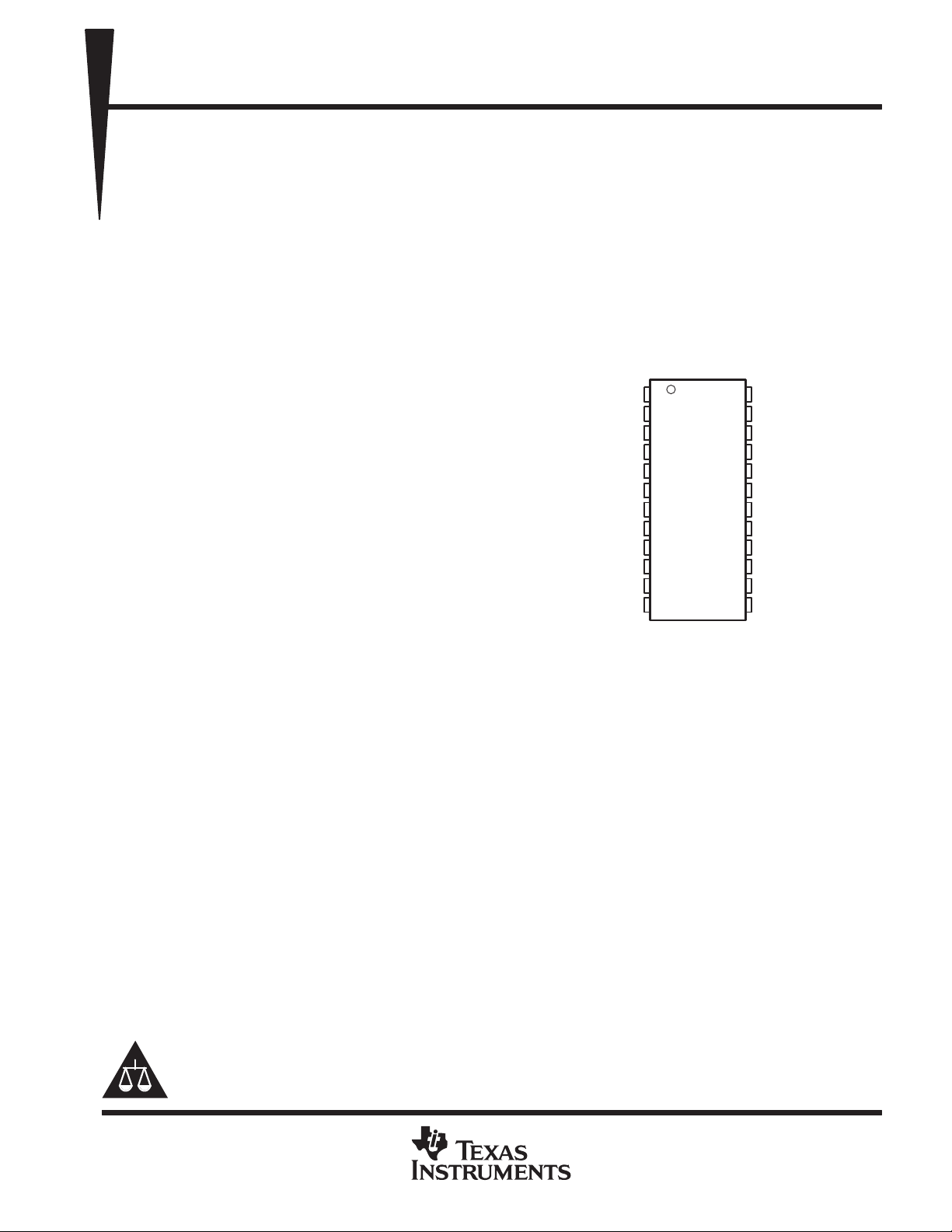
1
2
3
4
5
6
7
8
9
10
11
12
24
23
22
21
20
19
18
17
16
15
14
13
V
DD
REF
REFCLK
V
DD
P
GNDP
GND
LEADLAG
DLYCTRL
GNDPA
V
DD
PA
V
DD
PD
STOPB
PWRDNB
P0
P1
V
DD
O
GNDO
CLKOUT
NC
CLKOUTB
GNDO
V
DD
O
MULT0/DIV0
MULT1/DIV1
P2
DBQ PACKAGE
(TOP VIEW)
NC − No internal connection
Verzeichnis