

herunterladen

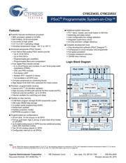
CY8C23433, CY8C23533
PSoC
®
Programmable System-on-Chip™
Cypress Semiconductor Corporation • 198 Champion Court • San Jose, CA 95134-1709 • 408-943-2600
Document Number: 001-44369 Rev. *I Revised January 29, 2015
Features
■ Powerful Harvard-architecture processor
❐ M8C processor speeds to 24 MHz
❐ 8x8 multiply, 32-bit accumulate
❐ Low power at high speed
❐ 3.0 V to 5.25 V operating voltage
❐ Industrial temperature range: –40 °C to +85 °C
■ Advanced peripherals (PSoC blocks)
❐ Four Rail-to-Rail analog PSoC blocks provide:
• Up to 14-bit ADCs
• Up to 8-bit DACs
• Programmable gain amplifiers
• Programmable filters and comparators
❐ Four digital PSoC blocks provide:
• 8- to 32-bit timers and counters, 8- and 16-bit pulse-width
modulators (PWMs)
• CRC and PRS modules
• Full-duplex UART
• Multiple SPI masters or slaves
• Connectable to all GPIO pins
❐ Complex peripherals by combining blocks
❐ High-Speed 8-bit SAR ADC optimized for motor control
■ Precision, programmable clocking
❐ Internal ±5%
[1]
24-/48-MHz oscillator
❐ High-accuracy 24 MHz with optional 32-KHz crystal and PLL
❐ Optional external oscillator, up to 24 MHz
❐ Internal oscillator for watchdog and sleep
■ Flexible on-chip memory
❐ 8 KB flash program storage 50,000 erase/write cycles
❐ 256 bytes SRAM data storage
❐ In-system serial programming (ISSP)
❐ Partial flash updates
❐ Flexible protection modes
❐ EEPROM emulation in flash
■ Programmable pin configurations
❐ 25-mA Sink, 10-mA source on all GPIO
❐ Pull-up, pull-down, high Z, strong, or open drain drive modes
on all GPIO
❐ Up to eight analog inputs on GPIO plus two additional analog
inputs with restricted routing
❐ Two 30-mA analog outputs on GPIO
❐ Configurable interrupt on all GPIOs
■ Additional system resources
❐ I
2
C slave, master, and multi-master to 400 kHz
❐ Watchdog and sleep timers
❐ User-configurable low voltage detection
❐ Integrated supervisory circuit
❐ On-chip precision voltage reference
■ Complete development tools
❐ Free development software (PSoC Designer™)
❐ Full-featured in-circuit emulator and programmer
❐ Full speed emulation
❐ Complex breakpoint structure
❐ 128-KB trace memory
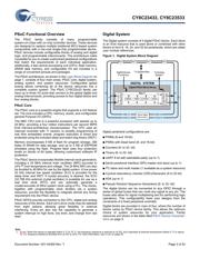
DIGITAL SYSTEM
SRAM
256 Bytes
Interrupt
Controller
Sleep and
Watchdog
Multiple Clock Sources
(Includes IMO, ILO, PLL, and ECO)
Global Digital Interconnect
Global Analog Interconnect
PSoC CORE
CPU Core (M8C)
SROM Flash 8K
Digital
Block
Array
Multiply
Accum.
Internal
Vol ta g e
Ref.
Digital
Clocks
POR and LVD
System Resets
Decimator
SYSTEM RESOURCES
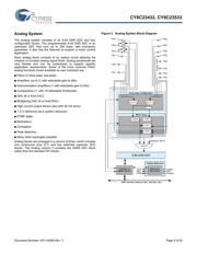
ANALOG SYSTEM
Analog
Ref
Analog
Input
Muxi n g
I
2
C
Por t 2 Por t 1 Po r t 0
Analog
Dr iv ers
System Bus
Analo g
Block Array
1 Row
4 Blocks
2 Columns
4 Blocks
SAR8 ADC
Por t 3
Logic Block Diagram
Note
1. Errata: When the device is operated within 0 °C to 70 °C, the frequency tolerance is reduced to ±2.5%, but if operated at extreme temperature (below 0 °C or above
70 °C), frequency tolerance deviates from ±2.5% to ±5%. For more information, see Errata on page 50.
Verzeichnis
- ・ Konfiguration des Pinbelegungsdiagramms on Seite 9 Seite 10
- ・ Teilenummerierungssystem on Seite 42 Seite 50
- ・ Blockdiagramm on Seite 1 Seite 3 Seite 4
- ・ Schweißen Temperatur on Seite 41
- ・ Beschreibung der Funktionen on Seite 35 Seite 42
- ・ Technische Daten on Seite 14 Seite 15 Seite 16 Seite 17 Seite 18
- ・ Elektrische Spezifikation on Seite 14 Seite 16 Seite 30
- ・ Teilenummernliste on Seite 50