

herunterladen
CY8C24094, CY8C24794
CY8C24894, CY8C24994
PSoC
®
Programmable System-on-Chip™
Cypress Semiconductor Corporation • 198 Champion Court • San Jose, CA 95134-1709 • 408-943-2600
Document Number: 38-12018 Rev. *O Revised June 11, 2009
1. Features
■ XRES Pin to Support In-System Serial Programming (ISSP)
and External Reset Control in CY8C24894
■ Powerful Harvard Architecture Processor
❐ M8C Processor Speeds to 24 MHz
❐ Two 8x8 Multiply, 32-Bit Accumulate
❐ Low Power at High Speed
❐ 3V to 5.25V Operating Voltage
❐ Industrial Temperature Range: -40°C to +85°C
❐ USB Temperature Range: -10°C to +85°C
■ Advanced Peripherals (PSoC
®
Blocks)
❐ 6 Rail-to-Rail Analog PSoC Blocks Provide:
• Up to 14-Bit ADCs
• Up to 9-Bit DACs
• Programmable Gain Amplifiers
• Programmable Filters and Comparators
❐ Four Digital PSoC Blocks Provide:
• 8 to 32-Bit Timers, Counters, and PWMs
• CRC and PRS Modules
• Full-Duplex UART
• Multiple SPI™ Masters or Slaves
• Connectable to all GPI/O Pins
❐ Complex Peripherals by Combining Blocks
❐ Capacitive Sensing Application Capability
■ Full Speed USB (12 Mbps)
❐ Four Uni-Directional Endpoints
❐ One Bi-Directional Control Endpoint
❐ USB 2.0 Compliant
❐ Dedicated 256 Byte Buffer
❐ No External Crystal Required
■ Flexible On-Chip Memory
❐ 16K Flash Program Storage 50,000 Erase and Write Cycles
❐ 1K SRAM Data Storage
❐ In-System Serial Programming (ISSP)
❐ Partial Flash Updates
❐ Flexible Protection Modes
❐ EEPROM Emulation in Flash
■ Programmable Pin Configurations
❐ 25 mA Sink, 10 mA Drive on all GPI/O
❐ Pull Up, Pull Down, High Z, Strong, or Open Drain Drive
Modes on all GPI/O
❐ Up to 48 Analog Inputs on GPI/O
❐ Two 33 mA Analog Outputs on GPI/O
❐ Configurable Interrupt on all GPI/O
■ Precision, Programmable Clocking
❐ Internal ±4% 24 and 48 MHz Oscillator
❐ Internal Oscillator for Watchdog and Sleep
❐ 0.25% Accuracy for USB with no External Components
■ Additional System Resources
❐ I
2
C Slave, Master, and Multi-Master to 400 kHz
❐ Watchdog and Sleep Timers
❐ User Configurable Low Voltage Detection
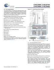
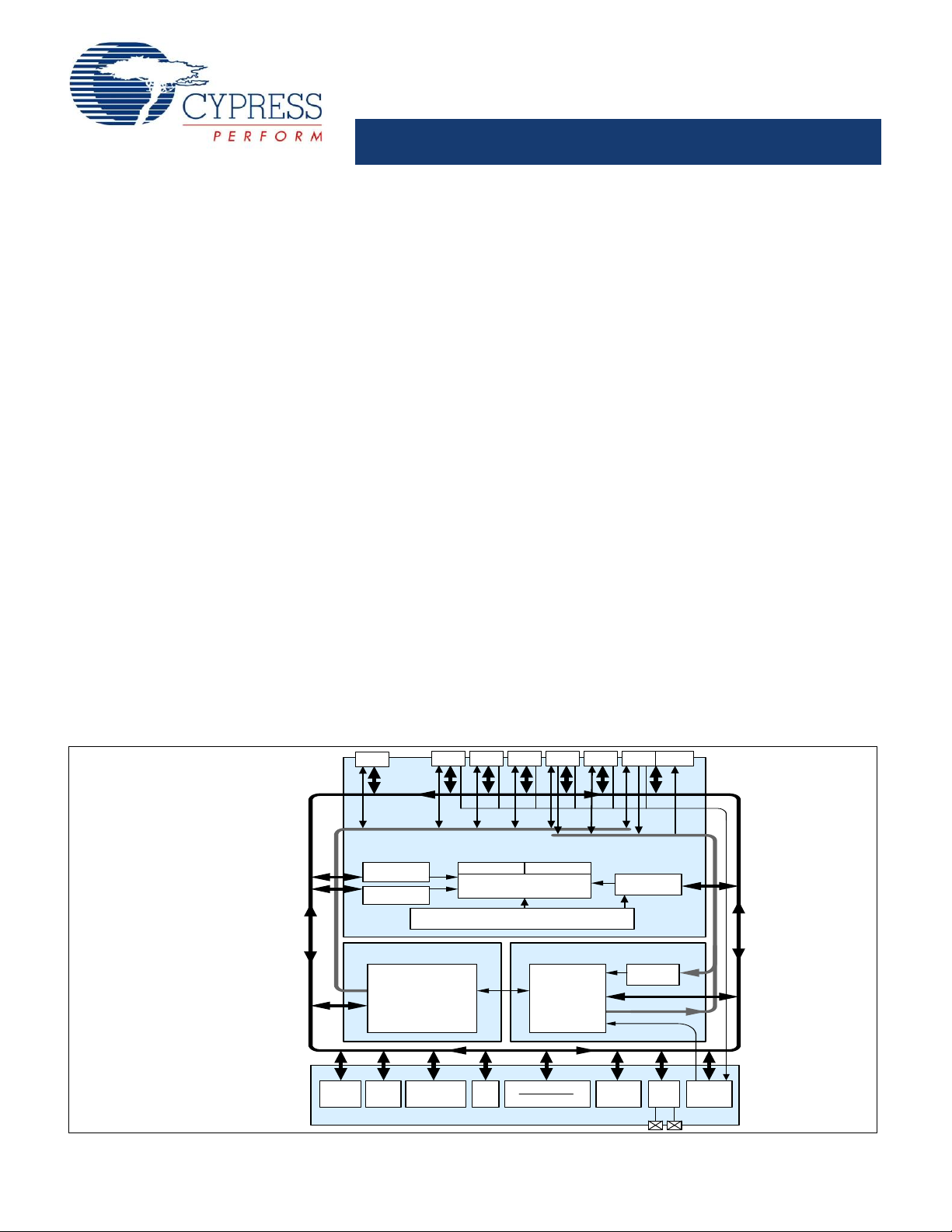
DIGITAL SYSTEM
SRAM
1K
Interrupt
Controller
Sleep and
W atchdog
Clock S ources
(Includes IM O and ILO )
Global Digital Interconnect
Global Analog Interconnect
PSoC CORE
CPU Core (M8C)
SROM Flash 16K
Digital
Block
A rray
Digital
Clocks
SYSTEM RESOURCES
ANALOG SYSTEM
Analog
Ref.
Port 5 Port 4 Port 3 Port 2 Port 1 Port 0
Analog
Drivers
Analog
Block
Array
In te rn a l
Voltage
Ref.
POR and LVD
System Resets
2
MACs
Decimator
Type 2
I2 C USB
Port 7
S
y
s
t
e
m
B
u
s
Analog
Input
Muxing
2. Logic Block Diagram
[+] Feedback
Verzeichnis
- ・ Konfiguration des Pinbelegungsdiagramms on Seite 1
- ・ Teilenummerierungssystem on Seite 44 Seite 45
- ・ Blockdiagramm on Seite 1 Seite 2 Seite 3
- ・ Schweißen Temperatur on Seite 41
- ・ Beschreibung der Funktionen on Seite 34 Seite 44
- ・ Technische Daten on Seite 7 Seite 20 Seite 21 Seite 22 Seite 23
- ・ Anwendungsbereich on Seite 35 Seite 44
- ・ Elektrische Spezifikation on Seite 7 Seite 20 Seite 22 Seite 30