
herunterladen

PSoC
®
5: CY8C53 Family Datasheet
Programmable System-on-Chip (PSoC
®
)
Cypress Semiconductor Corporation • 198 Champion Court • San Jose, CA 95134-1709 • 408-943-2600
Document Number: 001-66237 Rev. *D Revised February 15, 2012
General Description
With its unique array of configurable blocks, PSoC
®
5 is a true system level solution providing microcontroller unit (MCU), memory,
analog, and digital peripheral functions in a single chip. The CY8C53 family offers a modern method of signal acquisition, signal
processing, and control with high accuracy, high bandwidth, and high flexibility. Analog capability spans the range from thermocouples
(near DC voltages) to ultrasonic signals. The CY8C53 family can handle dozens of data acquisition channels and analog inputs on
every GPIO pin. The CY8C53 family is also a high-performance configurable digital system with some part numbers including
interfaces such as USB and multi-master I
2
C. In addition to communication interfaces, the CY8C53 family has an easy to configure
logic array, flexible routing to all I/O pins, and a high-performance 32-bit ARM
®
Cortex™-M3 microprocessor core. Designers can
easily create system-level designs using a rich library of prebuilt components and boolean primitives using PSoC
®
Creator™, a
hierarchical schematic design entry tool. The CY8C53 family provides unparalleled opportunities for analog and digital bill of materials
integration while easily accommodating last minute design changes through simple firmware updates.
Features
32-bit ARM Cortex-M3 CPU core
DC to 67 MHz operation
Flash program memory, up to 256 KB, 100,000 write cycles,
20-year retention, multiple security features
Up to 64 KB SRAM memory
128 bytes of cache memory
2-KB electrically erasable programmable read-only memory
(EEPROM) memory, 1 million cycles, and 20 years retention
24-channel direct memory access (DMA) with multilayer
AMBA high-performance bus (AHB) bus access
• Programmable chained descriptors and priorities
• High bandwidth 32-bit transfer support
Low voltage, ultra low power
Operating voltage range: 2.7 V to 5.5 V
6 mA at 6 MHz
Low power modes including:
• 2-µA sleep mode
• 300-nA hibernate mode with RAM retention
Versatile I/O system
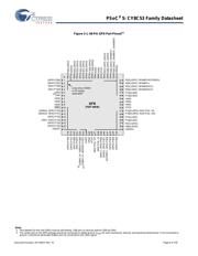
46 to 70 I/Os (60 GPIOs, 8 SIOs, 2 USBIOs))
Any GPIO to any digital or analog peripheral routability
LCD direct drive from any GPIO, up to 46x16 segments
CapSense
®
support from any GPIO
[1]
1.2 V to 5.5 V I/O interface voltages, up to 4 domains
Maskable, independent IRQ on any pin or port
Schmitt-trigger transistor-transistor logic (TTL) inputs
All GPIOs configurable as open drain high/low,
pull-up/pull-down, High-Z, or strong output
25 mA sink on SIO
Digital peripherals
20 to 24 programmable logic device (PLD) based universal
digital blocks (UDBs)
Full-Speed (FS) USB 2.0 12 Mbps using a 24 MHz external
oscillator
Up to four 16-bit configurable timer, counter, and PWM blocks
Library of standard peripherals
• 8-, 16-, 24-, and 32-bit timers, counters, and PWMs
• SPI, UART, and I
2
C
• Many others available in catalog
Library of advanced peripherals
• Cyclic redundancy check (CRC)
• Pseudo random sequence (PRS) generator
• Local interconnect network (LIN) bus 2.0
• Quadrature decoder
Analog peripherals (2.7 V V
DDA
5.5 V)
1.024 V ±1% internal voltage reference
Successive approximation register (SAR) analog-to-digital
converter (ADC), 12-bit at 700 ksps
Two 8-bit 5.5 Msps current digital-to-analog converters
(DAC) (IDACs) or 1 Msps voltage DACs (VDACs)
Four comparators with 95-ns response time
Two uncommitted opamps with 10-mA drive capability
Two configurable multifunction analog blocks. Example
configurations are programmable gain amplifier (PGA),
transimpedance amplifier (TIA), mixer, and sample and hold
CapSense support
Programming, debug, and trace
Serial wire debug (SWD) and single-wire viewer (SWV)
interfaces
Cortex-M3 flash patch and breakpoint (FPB) block
Cortex-M3 data watchpoint and trace (DWT) generates data
trace information
Cortex-M3 instrumentation trace macrocell (ITM) can be
used for printf-style debugging
DWT and ITM blocks communicate with off-chip debug and
trace systems via the SWV interface
Bootloader programming supportable through I
2
C, SPI,
UART, USB, and other interfaces
Precision, programmable clocking
3 to 48 MHz internal oscillator over full temperature and
voltage range
4 to 25 MHz crystal oscillator for crystal PPM accuracy
Internal PLL clock generation up to 67 MHz
32.768 kHz watch crystal oscillator
Low power internal oscillator at 1, 33, and 100 kHz
Temperature and packaging
-40°C to +85°C degrees industrial temperature
68-pin QFN and 100-pin TQFP package options
Note
1. GPIOs with opamp outputs are not recommended for use with CapSense.
Verzeichnis
- ・ Konfiguration des Pinbelegungsdiagramms on Seite 9 Seite 74
- ・ Abmessungen des Paketumrisses on Seite 98 Seite 99
- ・ Teilenummerierungssystem on Seite 96 Seite 97
- ・ Blockdiagramm on Seite 3 Seite 8 Seite 10 Seite 20 Seite 27
- ・ Typisches Anwendungsschaltbild on Seite 104
- ・ Schweißen Temperatur on Seite 98
- ・ Beschreibung der Funktionen on Seite 1 Seite 18 Seite 37 Seite 45 Seite 47
- ・ Technische Daten on Seite 31 Seite 57 Seite 58 Seite 59 Seite 60
- ・ Anwendungsbereich on Seite 53
- ・ Elektrische Spezifikation on Seite 57