

herunterladen
MUX & DEMUX - SMT
1
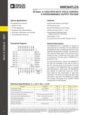
HMC847LC5
v06.1215
36 Gbps, 4:1 MUX WITH DUTY CYCLE CONTROL
& PROGRAMMABLE OUTPUT VOLTAGE
For price, delivery, and to place orders: Analog Devices, Inc.,
One Technology Way, P.O. Box 9106, Norwood, MA 02062-9106
Phone: 781-329-4700 • Order online at www.analog.com
Application Support: Phone: 1-800-ANALOG-D
Information furnished by Analog Devices is believed to be accurate and reliable. However, no
responsibility is assumed by Analog Devices for its use, nor for any infringements of patents or other
rights of third parties that may result from its use. Specications subject to change without notice. No
license is granted by implication or otherwise under any patent or patent rights of Analog Devices.
Trademarks and registered trademarks are the property of their respective owners.
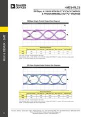
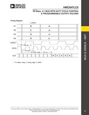
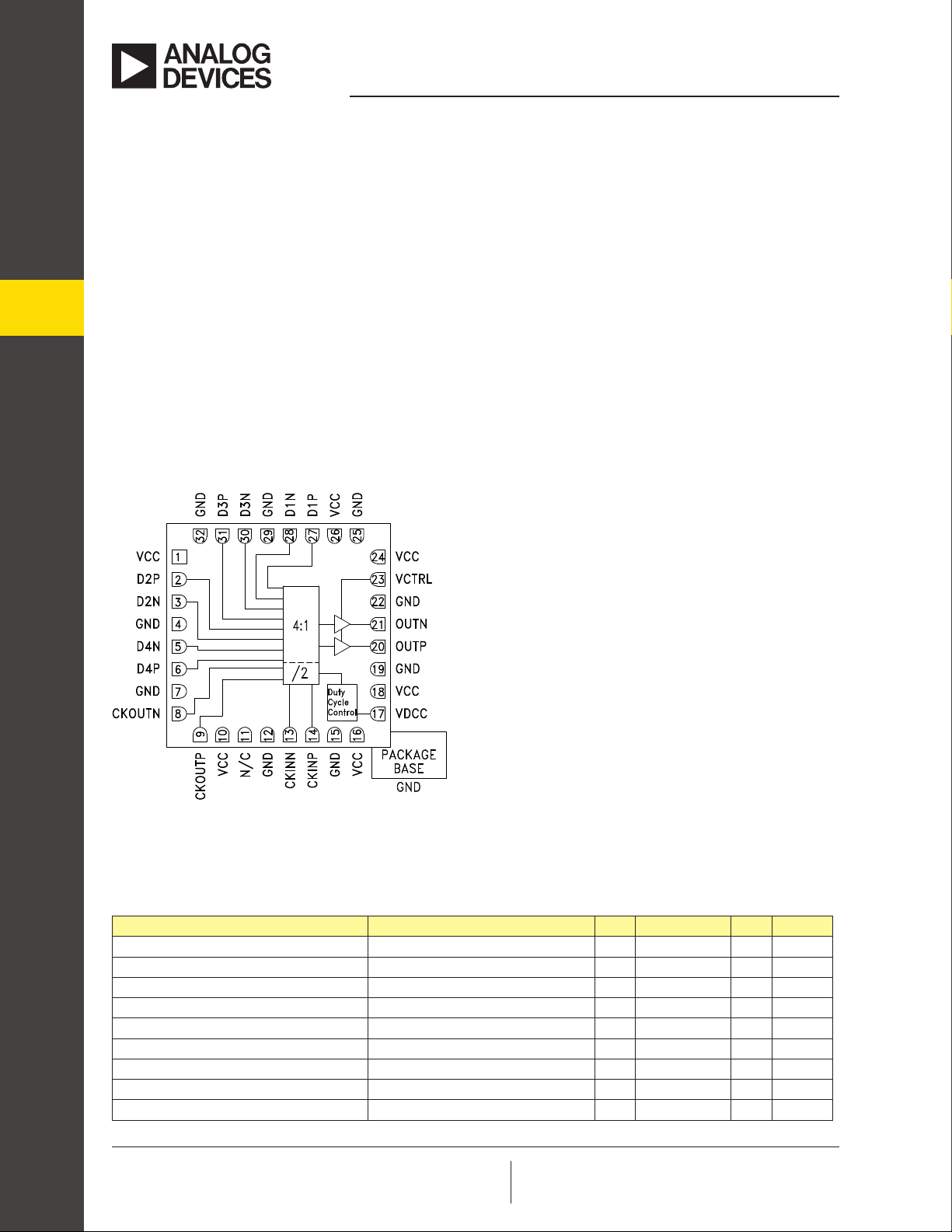
The HMC847LC5 is a 4:1 multiplexer for operation at
output data rate up to 36 Gbps. The mux latches the
four differential inputs on falling edge of the input clock
CKIN (See timing diagram on page.6). The device uses
both rising and falling edges of the half-rate clock to
serialize the data. A quarter-rate clock output, which
is synchronous to the data output of HMC847LC5, is
generated on chip.
All clock and data inputs / outputs of the HMC847LC5
are CML and terminated on-chip with 50 Ohms to
the, VCC, and may be DC or AC coupled. The inputs
and outputs of the HMC847LC5 may be operated
either differentially or single-ended. The HMC847LC5
also features an output level control pin, VCTRL,
which allows for loss compensation or signal level
optimization. The VDCC pin controls the data output
cross-point & duty cycle. The HMC847LC5 operates
from a single +3.3V supply and is available in ROHS
compliant 5x5 mm SMT package.
General Description
Features
Functional Diagram
Supports Data Rates up to 36 Gbps
Half Rate Clock Input
Quarter Rate Reference Clock Output
Fast Rise and Fall Times: 11 / 12 ps
Programmable Differential Output
Voltage Swing: 250 - 900 mVp-p
Single Supply: +3.3V
32 Lead Ceramic 5x5 mm SMT Package: 25 mm
2
Typical Applications
The HMC847LC5 is ideal for:
• SONET OC-768
• RF ATE Applications
• Broadband Test & Measurements
• Serial Data Transmission up to 36 Gbps
• High Speed DAC Interfacing
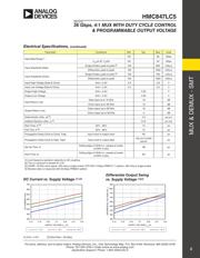
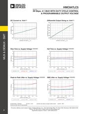
Electrical Specications, T
A
= +25°C, Vcc = +3.3V
Parameter Conditions Min. Typ. Max Units
Power Supply Voltage ± 5% Tolerance 3.13 3.3 3.47 V
Power Supply Current Vctrl = 2.5V 480 530 580 mA
Output Amplitude Control Voltage Range (Vctrl) 1.7 2.5 3 V
Data Output Voltage Swing Range Differential, peak-to-peak @ 36 Gbps 550 900 mVp-p
Duty Cycle Control Voltage Range (Vdcc) Vdcc = 1.6V for 50% duty cycle 1 1.6 2 V
Duty Cycle Control Range @ 36 Gbps 40 50 60 %
Clock Output Voltage Swing Differential, peak-to-peak @ 10 GHz 480 580 680 mVp-p
Maximum Data Rate 36 Gbps
Maximum Clock Rate Half Rate Clock 18 GHz
Verzeichnis
- ・ Konfiguration des Pinbelegungsdiagramms on Seite 8 Seite 9
- ・ Abmessungen des Paketumrisses on Seite 7
- ・ Markierungsinformationen on Seite 7
- ・ Blockdiagramm on Seite 8 Seite 9
- ・ Typisches Anwendungsschaltbild on Seite 1
- ・ Beschreibung der Funktionen on Seite 1 Seite 8 Seite 9
- ・ Technische Daten on Seite 7
- ・ Anwendungsbereich on Seite 1