


herunterladen
For price, delivery and to place orders: Hittite Microwave Corporation, 2 Elizabeth Drive, Chelmsford, MA 01824
Phone: 978-250-3343 Fax: 978-250-3373 Order On-line at www.hittite.com
Application Support: Phone: 978-250-3343 or apps@hittite.com
CLOCK DISTRIBUTION - SMT
1
HMC988LP3E
v04.1014
PROGRAMMABLE CLOCK DIVIDER AND DELAY
DC - 4 GHz
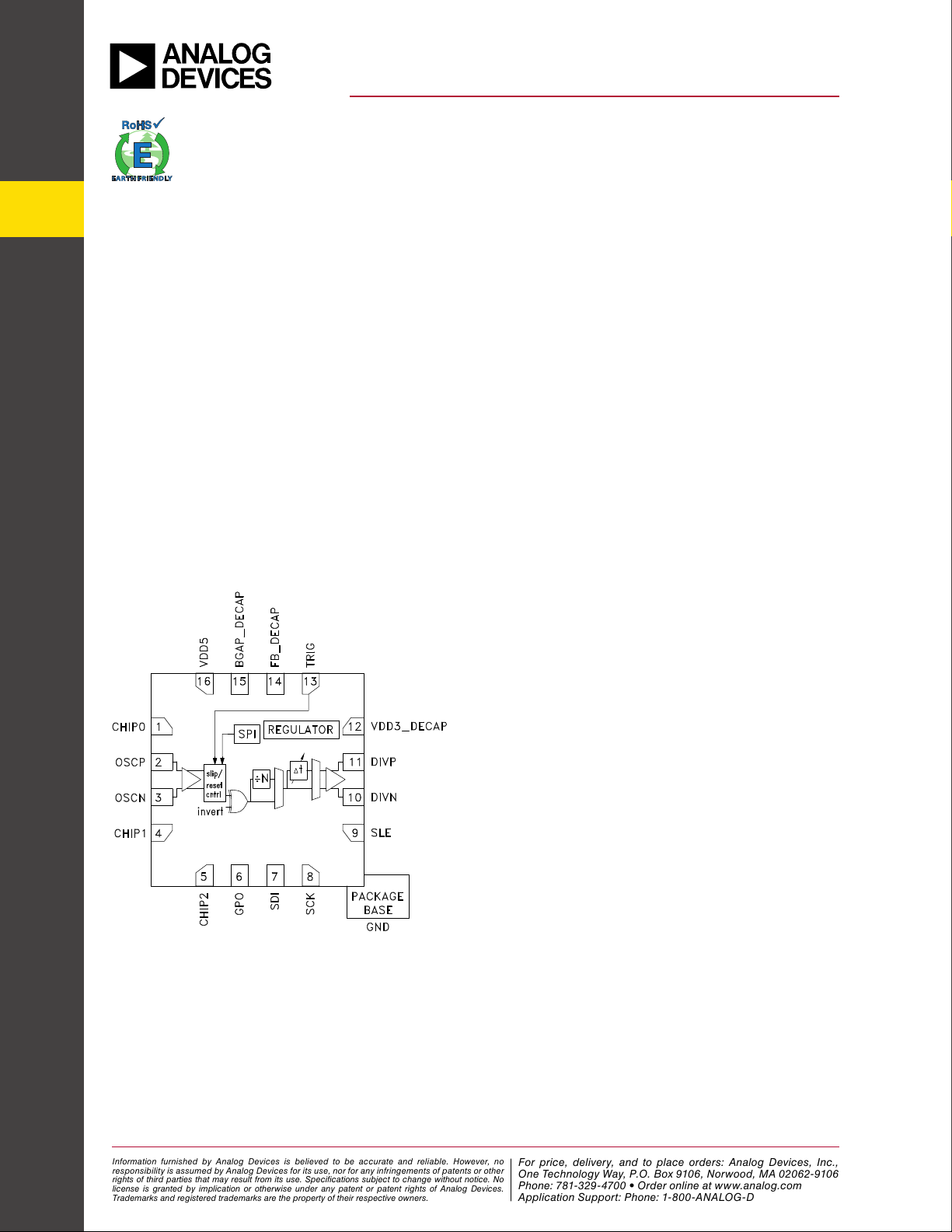
Functional Diagram
Typical Applications Features
General Description
The HMC988LP3E is ideal for:
• Basestation Digital Pre-Distortion Paths(DPD)
• High Performance Automated Test
Equipment(ATE)
• Backplane clock skew management
• Phase Coherence of multiple clock paths
• Clock Delay management to improve setup &
hold time margins
•
PCB signal ight time offset circuits
• Track and hold circuits for ADC/DACs
DC - 4 GHz
-170 dBc/Hz oor @ 100 MHz output
-164 dBc/Hz oor @ 2 GHz output
Integrated Jitter 35 fs
RMS
@ 100 MHz output
13 fs
RMS
(calculated) @ 2 GHz output
Adjustable output phase with soft/hard reset sync
Adjustable output delay in 60 steps of 20 ps
Flexible Input Interface:
LVPECL,LVDS,CML,CMOS Compatible
AC or DC Coupling
On - Chip Termination 50 Ω (100 Ω Differential)
Output Driver (LVPECL):
800 mVpp LVPECL into 50 Ω Single-Ended (+3
dBm Fo)
Up to 8 addressable dividers per SPI bus
3.3 V operation or 5 V operation with Optional on-
chip regulator for best performance
3 x 3 QFN Leadless SMT Package
The HMC988LP3E is a an ultra low noise clock
divider capable of dividing by 1/2/4/8/16/32. It is a
versatile device with additional functionality including
adjustable output phase, adjustable delay in 60 steps
of ~ 20 ps, a clock synchronization function, and a
clock invert option.
Housed in a compact 3x3 mm SMT QFN package, the
clock divider offers a high level of functionality. The
device works with 3.3 V supply or may be connected
to 5 V supply and utilize the optional on-chip regulator.
This on-chip regulator may be bypassed.
Up to 8 addressable HMC988LP3E devices can be
used together on the SPI bus.
The HMC988LP3E is ideally suited for data converter
applications with extremely low phase noise
requirements.
Information furnished by Analog Devices is believed to be accurate and reliable. However, no
responsibility is assumed by Analog Devices for its use, nor for any infringements of patents or other
rights of third parties that may result from its use. Specifications subject to change without notice. No
license is granted by implication or otherwise under any patent or patent rights of Analog Devices.
Trademarks and registered trademarks are the property of their respective owners.
For price, delivery, and to place orders: Analog Devices, Inc.,
One Technology Way, P.O. Box 9106, Norwood, MA 02062-9106
Phone: 781-329-4700 • Order online at www.analog.com
Application Support: Phone: 1-800-ANALOG-D
Verzeichnis
- ・ Konfiguration des Pinbelegungsdiagramms on Seite 7
- ・ Abmessungen des Paketumrisses on Seite 9
- ・ Markierungsinformationen on Seite 9
- ・ Blockdiagramm on Seite 10
- ・ Typisches Anwendungsschaltbild on Seite 1 Seite 12 Seite 15 Seite 16
- ・ Beschreibung der Funktionen on Seite 1 Seite 7
- ・ Technische Daten on Seite 1 Seite 3 Seite 4 Seite 5 Seite 6
- ・ Anwendungsbereich on Seite 1
- ・ Elektrische Spezifikation on Seite 5