
herunterladen
LTC6912
1
6912fa
FEATURES
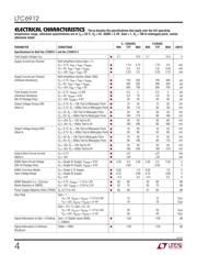
TYPICAL APPLICATIO
U
■
2 Channels with Independent Gain Control
LTC6912-1: (0, 1, 2, 5, 10, 20, 50, and 100V/V)
LTC6912-2: (0, 1, 2, 4, 8, 16, 32, and 64V/V)
■
Offset Voltage = 2mV Max (–40°C to 85°C)
■
Channel-to-Channel Gain Matching of 0.1dB Max
■
3-Wire SPI
TM
Interface
■
Extended Gain-Bandwidth at High Gains
■
Wired-OR Outputs Possible (2:1 Analog MUX
Function)
■
Low Power Hardware Shutdown (GN-16 Only,
2µA Max at 2.7V)
■
Rail-to-Rail Input Range
■
Rail-to-Rail Output Swing
■
Single or Dual Supply: 2.7V to 10.5V Total
■
Input Noise: 12.6nV/√Hz
■
Total System Dynamic Range to 115dB
■
16-Pin GN (SSOP) or 12-Pin DFN Package Options
■
Data Acquisition Systems
■
Dynamic Gain Changing
■
Automatic Ranging Circuits
■
Automatic Gain Control
Dual Programmable
Gain Amplifiers with
Serial Digital Interface
The LTC
®
6912 is a family of dual channel, low noise,
digitally programmable gain amplifiers (PGA) that are
easy to use and occupy very little PC board space. The
gains for both channels are independently programmable
using a 3-wire SPI interface to select voltage gains of 0, 1,
2, 5, 10, 20, 50, and 100V/V (LTC6912-1 ); and 0, 1, 2, 4,
8, 16, 32, and 64V/V (LTC6912-2). All gains are inverting.
The LTC6912 family consists of 2 matched amplifiers with
rail-to-rail outputs. When operated with unity gain, they
will also process rail-to-rail input signals. A half-supply
reference generated internally at the AGND pin supports
single power supply applications. Operating from single
or split supplies from 2.7V to 10.5V total, the LTC6912-X
family is offered in tiny SSOP and DFN-12 Packages.
, LTC and LT are registered trademarks of Linear Technology Corporation.
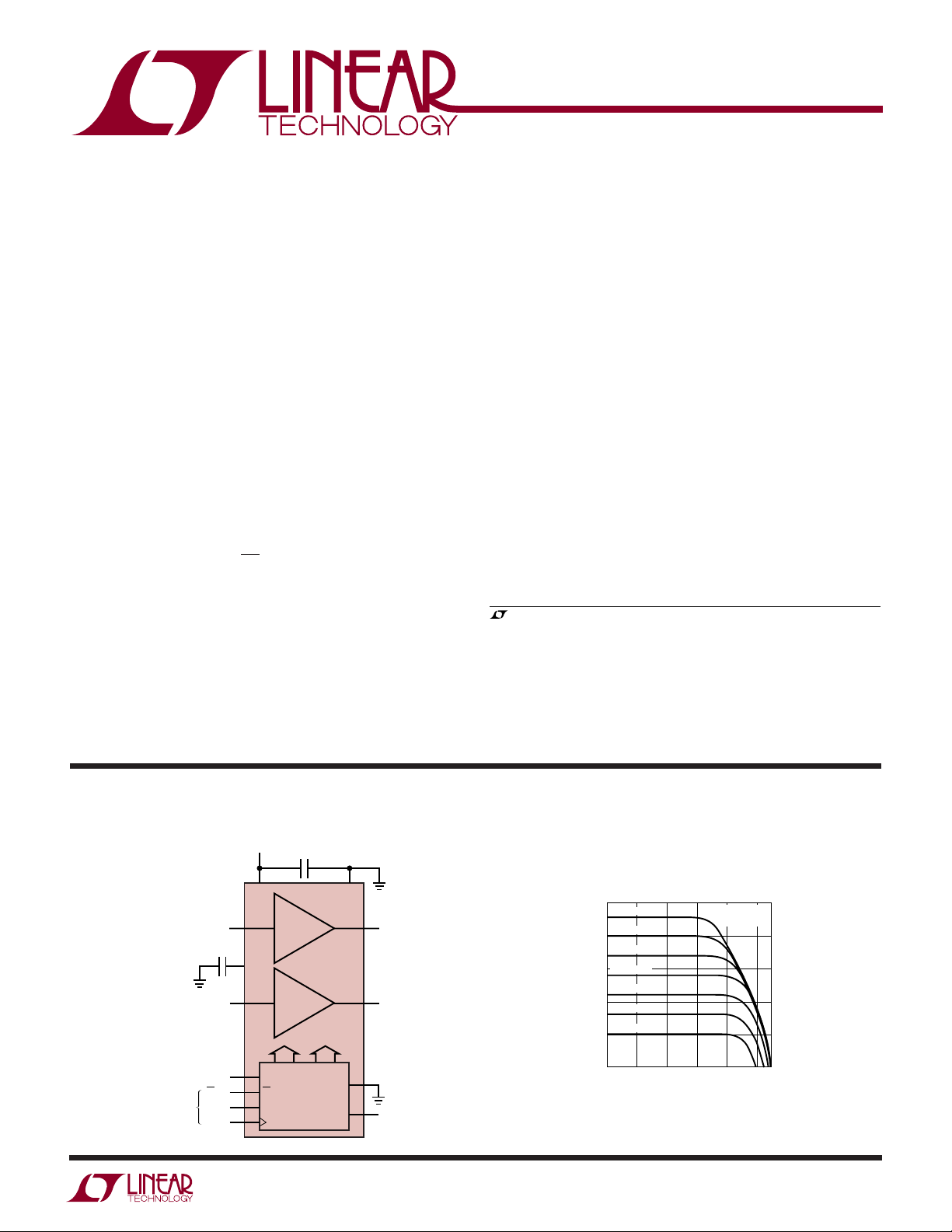
INA
AGND
INB
1µF
0.1µF
V
INA
V
INB
V
OUTA
= GAIN
A
• V
INA
V
OUTB
= GAIN
B
• V
INB
OUT A
OUT B
LTC6912-X
V
+
3V
V
–
SHDN
CS/LD
DATA
CLK
SHDN
CS/LD
D
IN
5
6
7
8
10
9
DGND
D
OUT
2
12 14
3
4
15
13
CHB CHA
3-WIRE
SPI
INTERFACE
6912 TA01a
FREQUENCY (kHz)
0.1
GAIN (dB)
40
30
20
10
0
–10
1
10 100 1000
6912 TA01b
10000
GAIN OF 64
GAIN OF 32
GAIN OF 16
GAIN OF 8
GAIN OF 4
GAIN OF 2
GAIN OF 1
V
S
= ±2.5V
V
IN
= 10mV
RMS
LTC6912-2
Frequency Response
A Dual, Matched Low Noise PGA (16-Lead SSOP Package)
DESCRIPTIO
U
All other trademarks are the property of their respective owners.
APPLICATIO S
U
Verzeichnis
- ・ Abmessungen des Paketumrisses on Seite 23
- ・ Paket-Footprint-Pad-Layout on Seite 23
- ・ Blockdiagramm on Seite 16 Seite 19 Seite 22
- ・ Beschreibung der Funktionen on Seite 19
- ・ Technische Daten on Seite 4 Seite 5 Seite 6 Seite 7 Seite 8
- ・ Anwendungsbereich on Seite 12
- ・ Elektrische Spezifikation on Seite 4 Seite 5 Seite 6 Seite 7 Seite 8