

herunterladen
© Semiconductor Components Industries, LLC, 2015
March, 2015 − Rev. 8
1 Publication Order Number:
NB4L7210/D
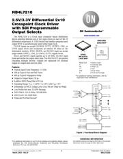
NB4L7210
2.5V/3.3V Differential 2x10
Crosspoint Clock Driver
with SDI Programmable
Output Selects
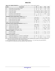
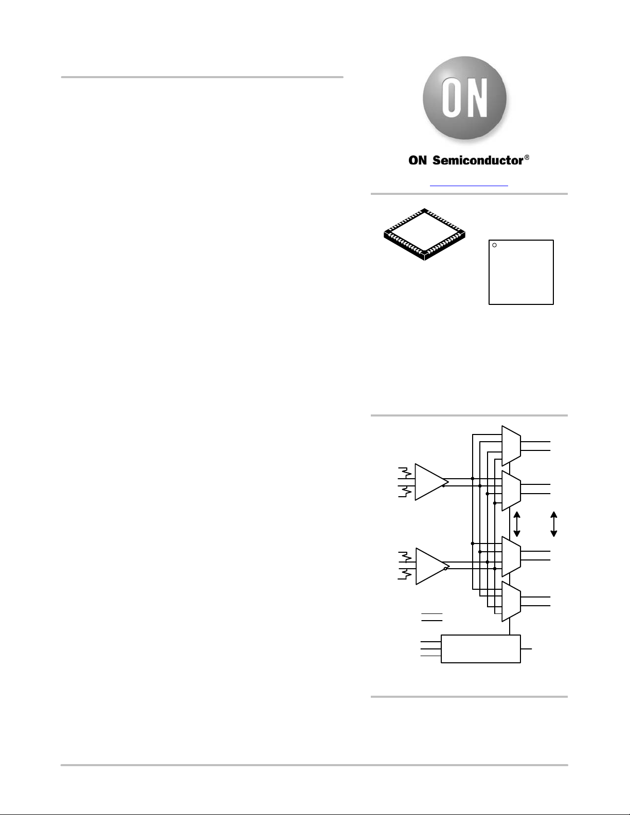
The NB4L7210 is a Clock input crosspoint fanout distribution
device selecting between one of two input clocks on each of the 10
differential output pairs. A 10 Bit Serial Data Interface programs each
output MUX to asynchronously select either Input clock.
CLOCK inputs can accept LVCMOS, LVTTL, LVPECL, CML, or
LVDS signal levels and incorporate an internal 50 ohms on die
termination resistors. SCLK, SDATA, and SLOAD input can accept
single ended LVPECL, CML, LVCMOS, LVTTL signals levels.
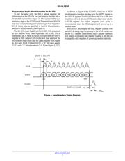
SCLK and SDATA inputs operate up to 20 MHz. SLOAD input
loads and latches the output select data. The SDATAOUT pin permits
cascading multiple devices. Outputs are optimized for minimal
output−to−output skew and low jitter.
Features
• Typical Input Clock Frequency > 2 GHz
• 200 ps Typical Rise and Fall Times
• 800 ps Typical Propagation Delay
• Output to Output Skew 150 ps
• Additive RMS Phase Jitter of 0.2 ps
• Operating Range: V
CC
= 2.375 V to 3.6 V with V
EE
= 0 V
• Differential LVPECL Output Level (Typ 700 mV Peak−to−Peak)
• Low Profile 8x8 mm, 52 QFN Package
• 10GE WAN: 155.52 MHz / 622.08 MHz
• 10GE LAN: 161.1328 MHz
• These are Pb−Free Devices*
*For additional information on our Pb−Free strategy and soldering details, please
download the ON Semiconductor Soldering and Mounting Techniques
Reference Manual, SOLDERRM/D.
*For additional marking information, refer to
Application Note AND8002/D.
MARKING
DIAGRAM*
QFN52
MN SUFFIX
CASE 485M
www.onsemi.com
See detailed ordering and shipping information in the package
dimensions section on page 10 of this data sheet.
ORDERING INFORMATION
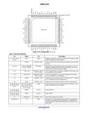
Figure 1. Functional Block Diagram
NB4L7210 = Device Code
A = Assembly Site
WL = Wafer Lot
YY = Year
WW = Work Week
G = Pb−Free Package
NB4L
7210
AWLYYWWG
1
52
152
CLK0
CLK0b
CLK1
CLK1b
V
TCLK0b
VTCLK0
V
TCLK1b
VTCLK1
Q0
SCLK
SDATA
SLOAD
VCC
VEE
SDATAOU
T
Q0
b
Q1
Q1
b
Q8
Q8
b
Q9
Q9
b
Verzeichnis
- ・ Konfiguration des Pinbelegungsdiagramms on Seite 2
- ・ Abmessungen des Paketumrisses on Seite 11
- ・ Paket-Footprint-Pad-Layout on Seite 11
- ・ Teilenummerierungssystem on Seite 1 Seite 10 Seite 11
- ・ Markierungsinformationen on Seite 1 Seite 11
- ・ Blockdiagramm on Seite 1
- ・ Technische Daten on Seite 10
- ・ Teilenummernliste on Seite 3